Fraunhofer Institute for Ceramic Technologies and Systems IKTS
Cost-effective copper-silicon nitride composites as circuit boards for power electronics
Current research
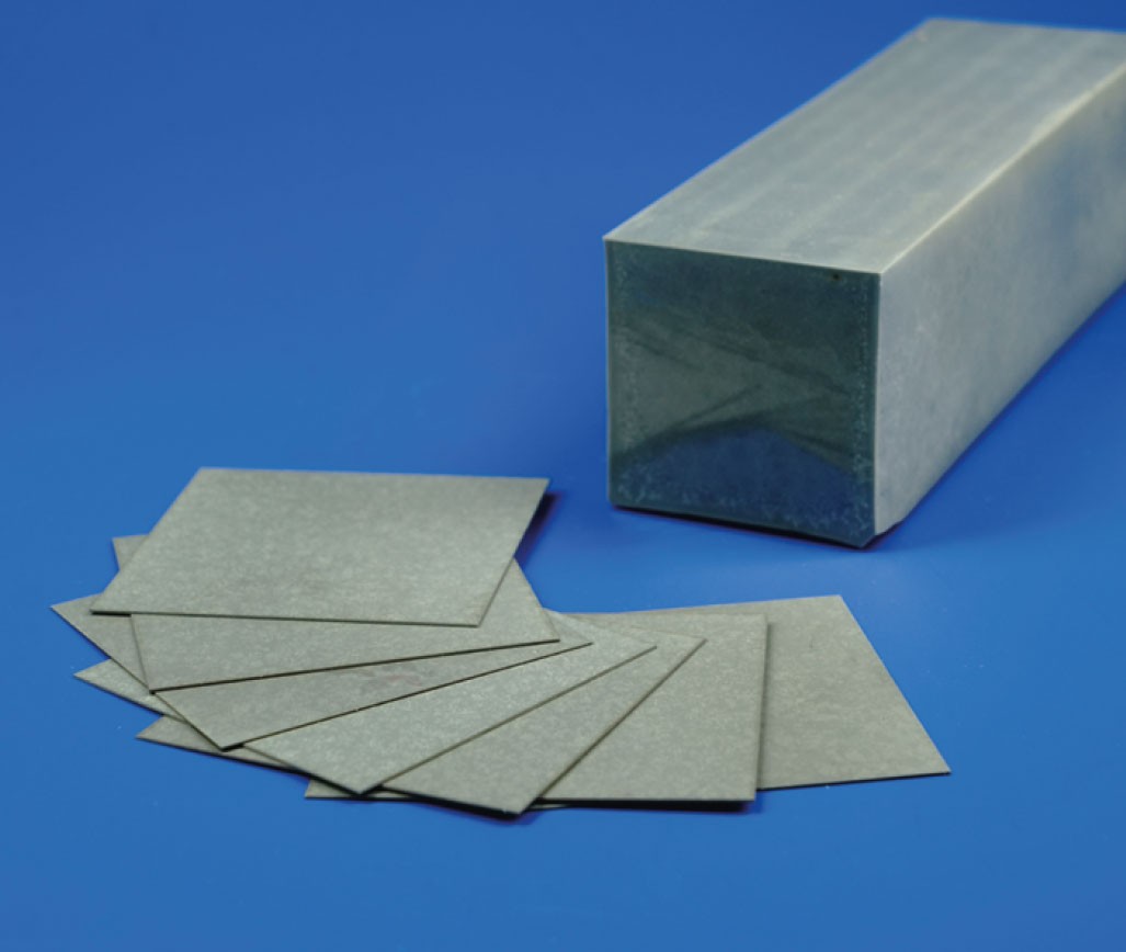
Si3N4 ceramic substrates produced by multi-wire sawing (2 x 2 inches).
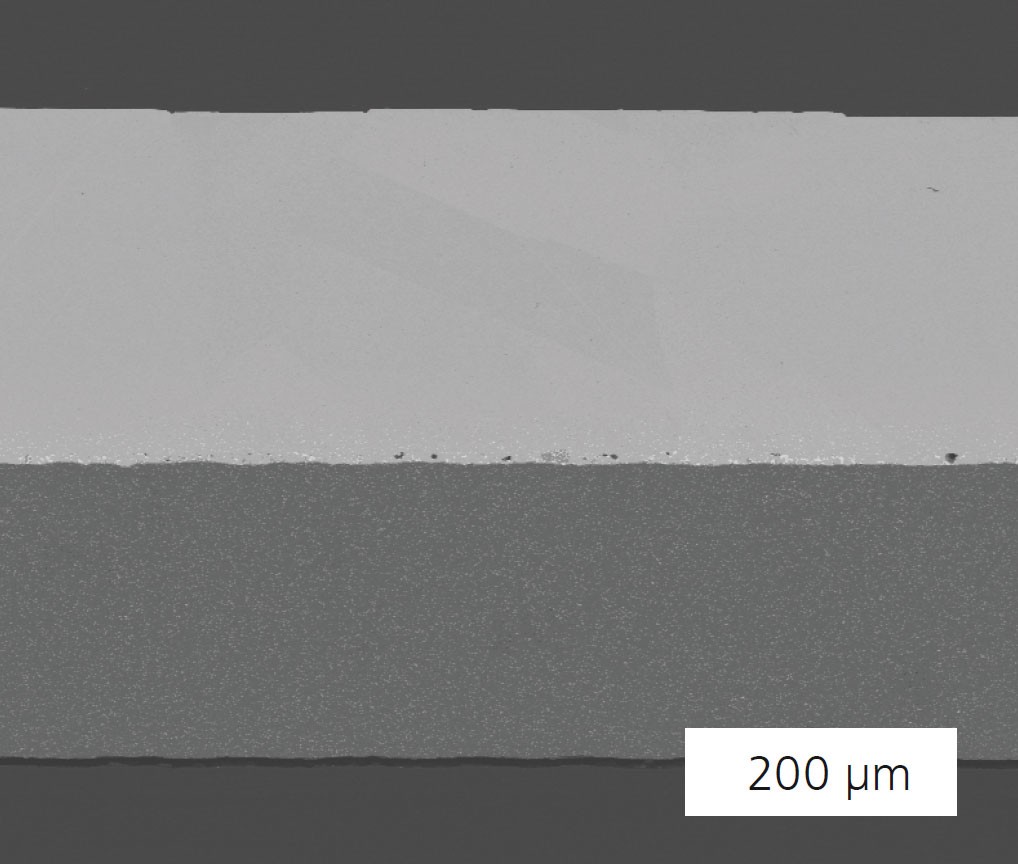
Joining zone of an active metal-brazed Cu-Si3N4 composite.

Measurement test setup with AMB-DUT (device under test) and PRPD-pattern (phase-resolved partial discharge).
Structured metal-ceramic substrates are an important component for power electronic components as circuit boards. Existing solutions such as directly bonded copper-aluminum oxide (DBC, direct bonded copper) or active metal-brazed copper-aluminum nitride substrates (AMB, active metal brazing) cannot meet the future requirements of electromobility and realize the full potential of new silicon carbide (SiC)-based semiconductor components. One solution might be composites with silicon nitride (Si3N4) ceramics with their superior mechanical properties. This enables metallized ceramic substrates to be used in power electronic assemblies with significantly improved stability against the active and passive thermal cycles.
In the joint project CuSiN, Fraunhofer IKTS and its partners are developing reliable and high-performance copper-silicon nitride (Cu-Si3N4) substrates using active metal brazing (AMB technology). Ceramic Si3N4 substrates with thicknesses < 320 μm made by means of multi-wire sawing of sintered Si3N4 blocks already show thermal conductivities > 90–100 W m-1 K-1 and strengths > 700 MPa (top image). The basis for this is particularly low-oxygen content Si3N4 powders in combination with aluminum-free additives. A project novelty is the possibility to sinter compact Si3N4 substrates with dimensions up to 5 x 7 inches to homogeneous and very low porous microstructures.
New filler metal brazing pastes suitable for automated screen printing are required for joining copper films to Si3N4 substrates by active brazing. In addition to good bond strengths (currently up to 25 N per mm copper width), the joining zones must be as pore-free as possible to ensure high reliability of the bonds (middle figure). This is achieved by paste formulations with homogeneously distributed, minimal proportions of active phases and active filler metal layers of less than 25 μm. Furthermore, a reliable removal of organic binder components from printed filler metal layers in planar Cu-Si3N4 assemblies is possible even in ultra-high vacuum below 380° C. The brazing process is optimized with regard to low-defect brazed filler metal zones, high bond strengths and minimized filler metal amounts.
In the field of characterization of active metal-brazed Cu-Si3N4 substrates, investigations of the partial discharge behavior require the development of new methodological approaches. Partial discharge measurement is a non-destructive characterization method for detecting defects in dielectrics. Customized measurement set-ups and analysis methods can record partial discharge processes with high temporal resolution and create an understanding of these effects by correlating them with material and substrates properties.
Based on the findings obtained within the framework of CuSiN, the field of offered services includes the development of Si3N4-ceramics, active filler metal pastes and active metal brazing processes as well as material specific and electrical characterization of copper-ceramic substrates.
Supported by