 Fraunhofer Institute for Ceramic Technologies and Systems IKTS
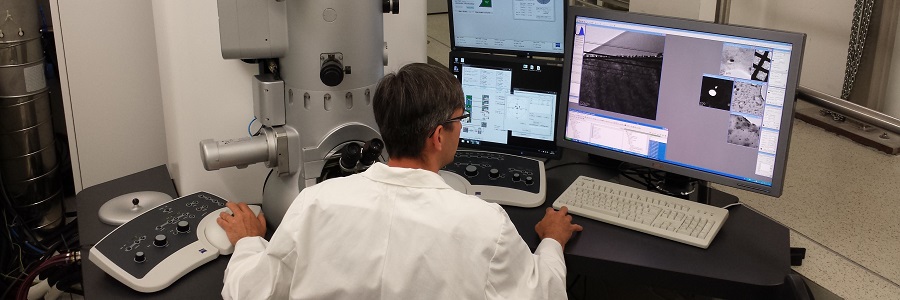
Microelectronic Materials and Nanoanalysis
Department
The nanoscale properties of materials and material systems determine the macroscale performance and reliability of components, functions and processes. Novel and complex material (systems) are therefore a key for innovations in micro-, nano- and optoelectronics, energy, environmental and medical (technology).
Having the right knowledge about the relevant structure-property relationships can accelerate the development of new products, specifically improve the reliability of components and increase the efficiency of technological processes. This requires a deep understanding of materials and their time-resolved interactions from the atomic to the millimeter scale.
The department "Microelectronic Materials and Nanoanalysis" of Fraunhofer IKTS offers a unique infrastructure of high-resolution electron, ion and X-ray microscopy to provide competent consulting, contract analysis and methodological developments to partners in industry and research. A special focus is on the combination and correlation of different methods as well as the customized development of unique testing technology.
Core competences are on the one hand high-resolution non-destructive X-ray tomography for the measurement of micro- and nanostructures as well as non-destructive defect localization in combination of electron, ion and X-ray microscopy with micro- and nanomechanical tests. On the other hand, physical failure analysis for the elucidation of damage and failure mechanisms in microelectronic devices is one of our specialties.
Through close networking with other Saxon Fraunhofer institutes in the Dresden Fraunhofer Cluster Nanoanalytics DFCNA as well as within the DRESDEN-concept alliance, research and development projects are carried out along the entire value and innovation chain from basic research to implementation in industry.
Services offered
- High-resolution and multiscale analysis of materials and microsystems
- Micro- and nanostructure characterization with microscopic and nanomechanical methods: scanning and transmission electron microscopy (SEM/TEM), ion fine beam analysis and preparation (gallium and Xe-FIB), X-ray microscopy and nanotomography, nanoindentation
- Basic research
- Reliability investigations in microelectronics (electromigration, CPI)
Cooperations
- Dresden Fraunhofer Cluster Nanoanalytics DFCNA