 Fraunhofer Institute for Ceramic Technologies and Systems IKTS
Multiscale 3D analytics, data correlation and preparation in semiconductor development
Current research
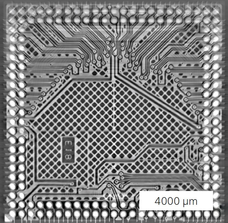
X-ray microscopy on a DRAM chip; overview scan with 8.6 μm voxel size.
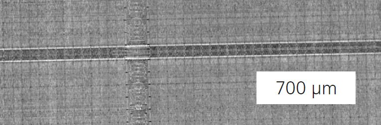
Zoom-In Detail aus oberem Bild.

Detailed scan with 0.6 μm voxel size.
Fraunhofer IKTS offers analytical and preparative workflows for cross-scale, multimodal analysis to support the development of materials, components and devices of micro- and power electronics, with the aim of accelerated optimization. Preparation can be inert and cooled (by liquid nitrogen) as required. The analytics provided includes microscopes (2D), which use electrons to image ions and light (including X-rays), as well as X-ray computer tomographs (3D). These devices are equipped with operando modules for mechanical testing (e.g. tension/pressure, bending, adhesion). All data generated in this way is stored according to FAIR (findable, accessible, interoperable, reachable) principles and is used for correlative, quantitative and statistical evaluation, including methods of machine learning, and made available to the customer.
Non-destructive volume analysis
Integrated semiconductor devices (semiconductor chip, image 1–4) can be tomographically examined using X-ray microscopy (XRM). Various such devices are available; they work with 3D volume pixels (so-called voxels) ranging from a few nanometers to a few 10 μm resolution. In contrast, the highly absorbent metallic traces and vertical contacts in particular become visible. Any defects such as damaged metallization can be identified and located in the volume. A target preparation for the defects can then be carried out and examined further through subsequent analysis.
Sample target preparation
Micro- and nanoanalysis usually requires dedicated sample target preparation, which is fully available at Fraunhofer IKTS and supports the analytics along the process chain. By means of laser ablation, mechanical polishing (TXP) and ion etching (TIC3X), encapsulations of components can be removed and internal surfaces can be gently exposed. Final preparation, accurate to the nanometer, takes place in the dual-beam scanning electron ion microscope (FIB-SEM), for which gallium, helium and neon ions are available.
Cross-scale, multi-modal and correlative analysis and data correlation
Analytical microscopy (composition determination with energy dispersive X-ray analysis – EDX) and spectroscopy (e.g. molecular fingerprinting with Raman spectroscopy and time-of-flight mass spectroscopy – TOF-MS with ion beam material removal in FIB-SEM) can provide a comprehensive picture of the morphology and multi-physical properties of samples. As part of the reliability analysis, IKTS can combine analytical microscopy in FIB-SEMs, including element and crystal analysis and electrical fault analysis using scanning probe methods, with mechanical testing (in FIB-SEM and XRM). Thanks to nanoGPS technology [1], it is possible to achieve relocation with μm accuracy of identical sample sites in the various measurement modalities. The complex, very large data sets (for XRM e.g. > 15 GB per data set) are automated, quantitatively and statistically evaluated using AI-based methods.
Literature
[1] O. Acher et al., Meas. Sci. Technol. 32, 045402 (2021).
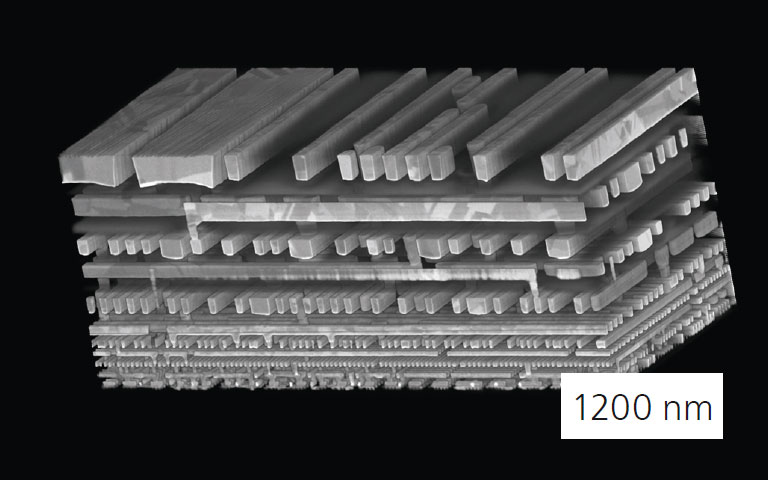
Detailed 3D view of a CPU chip with nm voxel size from a tomography generated with the focused Ga-ion beam in an electron microscope.