 Fraunhofer Institute for Ceramic Technologies and Systems IKTS
References and application examples
Ultrasonic biplanar arrays
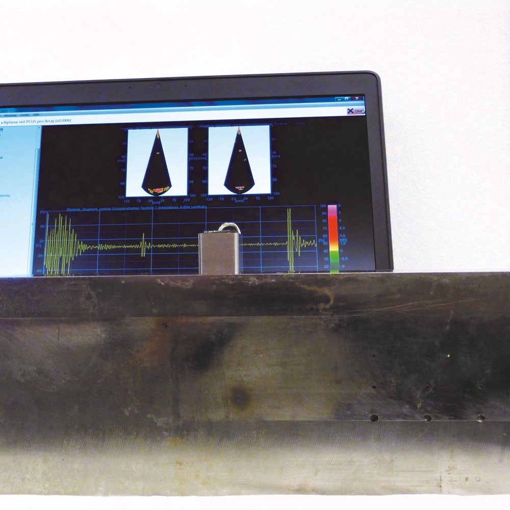
Biplanar array for ultrasound testing.
In ultrasonics, different sensor types based on single-element or array technology are used. Specifically for array technologies, hardware solutions with numerous synchronized channels are required; these solutions become increasingly expensive as the number of channels increases. Linear arrays are usually used in practice, but they are not sufficient in some cases. In such cases, matrix arrays represent an alternative, which, however, is very difficult to implement: an 8x8 matrix array alone requires 64-channel electronics.
Development of so-called biplanar arrays at Fraunhofer IKTS aims at reproducing the performance of a matrix array using two combined linear arrays aligned orthogonally to each other. Through appropriate switching of the connected electronics, various points in the two-dimensional space under the array can be activated to reproduce the imaging characteristics of a matrix array. The decisive advantage of this design is that it enables an 8x8 array to be reproduced with just 16 channels.
Ultrasonic systems for rail vehicles
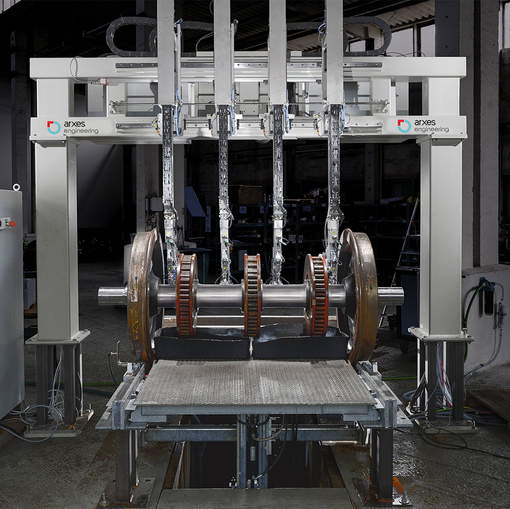
Fully automated phased-array ultrasonic test device for non-destructive testing of solid shaft gear sets in disassembled condition.
Highly loaded train and railroad car components such as axles and wheels need to be inspected regularly. Together with partners from industry, Fraunhofer IKTS is developing the software and electronics for ultrasonic testing systems. The software design enables intuitive operation by inspection personnel as well as mistake-proof inspection. Engineering standards are fully met. The powerful PCUS® pro electronics guarantee rapid testing and flexible parameterization due to the high data rates and the parallel FPGA design.
This work has led, for example, to the development of a hollow-shaft testing system for high-speed trains. With seven different single-element probes, the component can be inspected quickly and safely. In addition, a solid-shaft testing system for freight trains was developed using an ultrasonic phased array as a basis. The two systems have been used successfully both by Deutsche Bahn and outside Germany for a few years now.
EddyCus® Robot
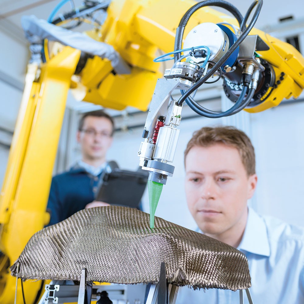
EddyCus Robots® for inspection of freeform-based components using high-frequency eddy current technology.
Carbon fiber composites are shaped into complex geometries early on in the production process. For this reason, the EddyCus® Robot for testing of carbon fiber preforms was developed on the basis of the high-frequency eddy current technology with 2D or 2.5D scanning systems for flat test specimens. The path plan for the robot-based testing system can be generated according to the CAD data.
However, in case the data are not available or are subject to strong fluctuations due to the manufacturing process, the EddyCus® Robot provides an alternative system. Here, an unknown part is digitized with a structured-light scanning camera through parametric path planning on the reconstructed surface. The sensor is then guided over the part surface orthogonally to the surface. At the end of the process, the sensor measurement results and the path data are combined to form a C scan. The EddyCus® Robot is currently being used, for example, at Bayerische Motoren Werke AG for the detection of fiber, layer, and other internal defects.
X-ray laminography system
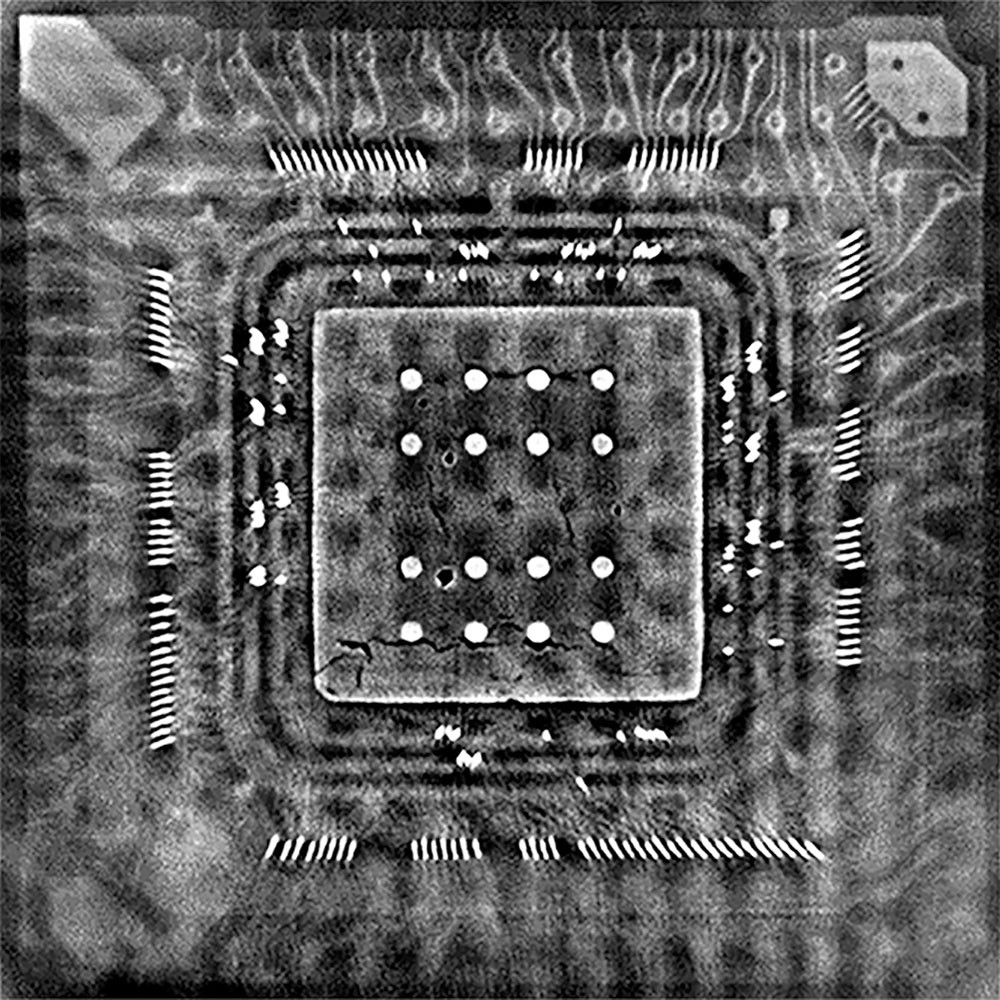
X-ray laminography image of a ball grid array with crack.
Inclusions in soldering points or small cracks can occur in the production of electronic devices. With conventional x-ray computed tomography, three-dimensional datasets representing the internal structure of a part can be generated. The resolution of the individual voxels strongly depends on the overall size of the test object. Hence, for large flat structures such as PCBs, only a limited resolution can be obtained.
To increase the resolution, Fraunhofer IKTS developed the so-called x-ray laminography method. Through a very specific arrangement of x-ray tube, detector, and object, a high-resolution 3D dataset can be generated especially for small subareas of flat component assemblies. In this way, cracks in bond pads for mounting electronic components on substrates can be quickly visualized in a non-destructive manner without the need for preparation.
The method is typically used in electronics fabrication, but use in quality assurance of embedded systems in CFRP structures is gaining momentum.