 Fraunhofer Institute for Ceramic Technologies and Systems IKTS
Microelectronic materials and nanoanalytics for improved performance and reliability
Current research
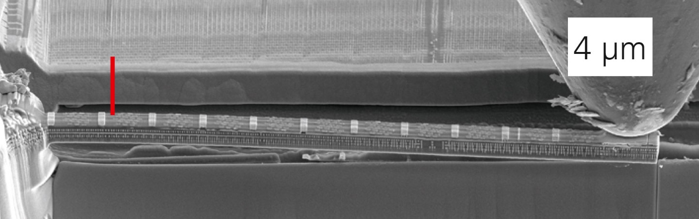
HR-TEM micrograph of a transistor structure with atomic resolution of the transistor.
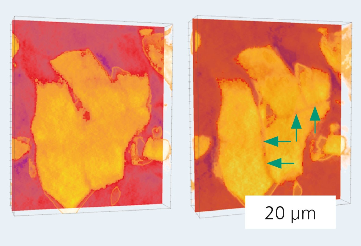
X-ray tomographic 3D microscopy of a heterogeneous mold compound material.
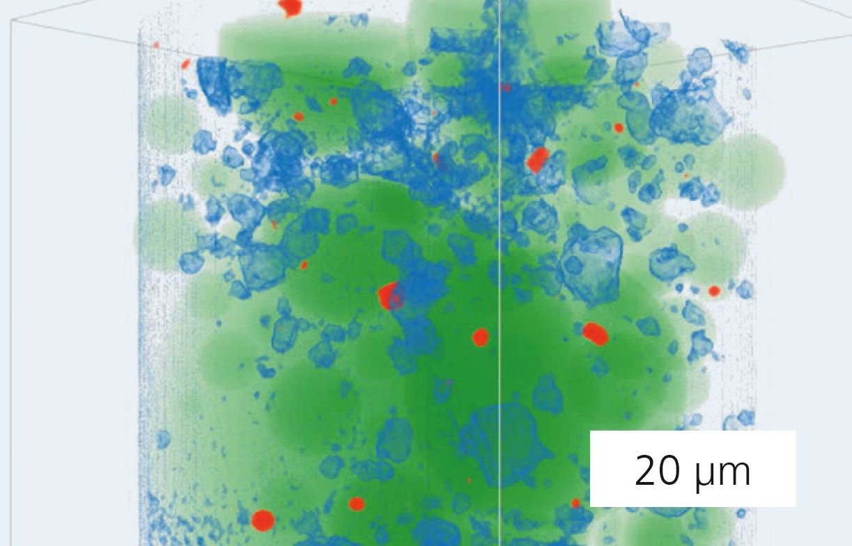
Operando X-ray microscopy experiment on an active battery cell, left: cathode particles before cell cycling, right: crack formation after 37 cycles.
New and complex materials systems are the key to innovation in micro-, nano- and optoelectronics as well as energy, environmental and medical technology. Most of the macroscopic properties of materials and structural systems stem from the microscopic world. The correct knowledge of relevant relationships between structures and properties can speed up the development of new products, improve the reliability of components in a targeted way and increase the efficiency of technological processes.
The Microelectronic Materials and Nanoanalytics department at Fraunhofer IKTS is deeply engaged in cutting-edge nanoanalytical methods as well as innovative, problem-specific experimental designs in microscopes to make microscopic effects observable and further exploit the measured data. One particular focal point is the combination of processes and the observation of time-resolved interactions.
Microelectronics is an important field of application. In close cooperation with industry, the department addresses questions on the chip level, reaching down in scale from micrometers to a few nanometers. The portfolio of methods includes:
- High-resolution analytical transmission electron microscopy (HR-TEM including EDX and EELS)
- High-resolution X-ray nanotomography (nXCT)
- Scanning electron microscopy/plasma-FIB (SEM/FIB) for flexible sample preparation as well as EDX/EBSD for chemical and crystallographic characterization
- Cutting-edge nanomechanical test systems (e.g. nanoindentation)
These methods can, for example, be used for the high-resolution imaging of transistor structures and their failure modes down to the atomic scale (top figure) or of heterogeneous materials in 3D with resolutions of several 10 nm (second figure). This facilitates a considerably deeper insight into the structure and behavior of microelectronic materials.
In addition to imaging methods, the department is working intensively to understand and optimize issues of reliability, such as electromigration, thermomechanical reliability and radar frequency behavior. Relevant equipment is at hand, for instance a radio frequency wafer prober and EM testing ovens.
Moreover, the integration of experiments inside microscopes, meaning the assembly of in-situ and operando tests, for instance for microelectronic or energy systems, is part of the department’s core expertise. The assembly of an active battery cell in the nXCT is one example of an innovative realization of operando experiments in X-ray microscopy. The setup allows to investigate microscopic crack formation in cathode particles during cell cycling (third figure). Additionally, in-situ experiments in microscopes provide insightful information. For example, the system E-modulus of a nanostructured microelectronics sample can be determined in situ in a scanning electron microscope (bottom image).
In-situ SEM nanomechanics cantilever experiment on a nanostructured microelectronics specimen.