
Stress effects in transistors
In microelectronic technologies, local mechanical stress is used to enhance performance and efficiency. The phenomenon known as ‘piezoresistive effect’ leads to improved electrical performance. However, uncontrolled thermo-mechanical stress can affect the functionality and reliability of microelectronic devices in harsh environments, for instance in cars. An established technique to estimate the influence of stress on device performance under stress is four-point bending. But this method only allows the application of homogeneous global stress. In order to determine the local influence of stress effects with a high resolution, a novel technique for localized loading based on non-destructive indentation was developed and successfully implemented at Fraunhofer IKTS .
Non-destructive indentation on test chips
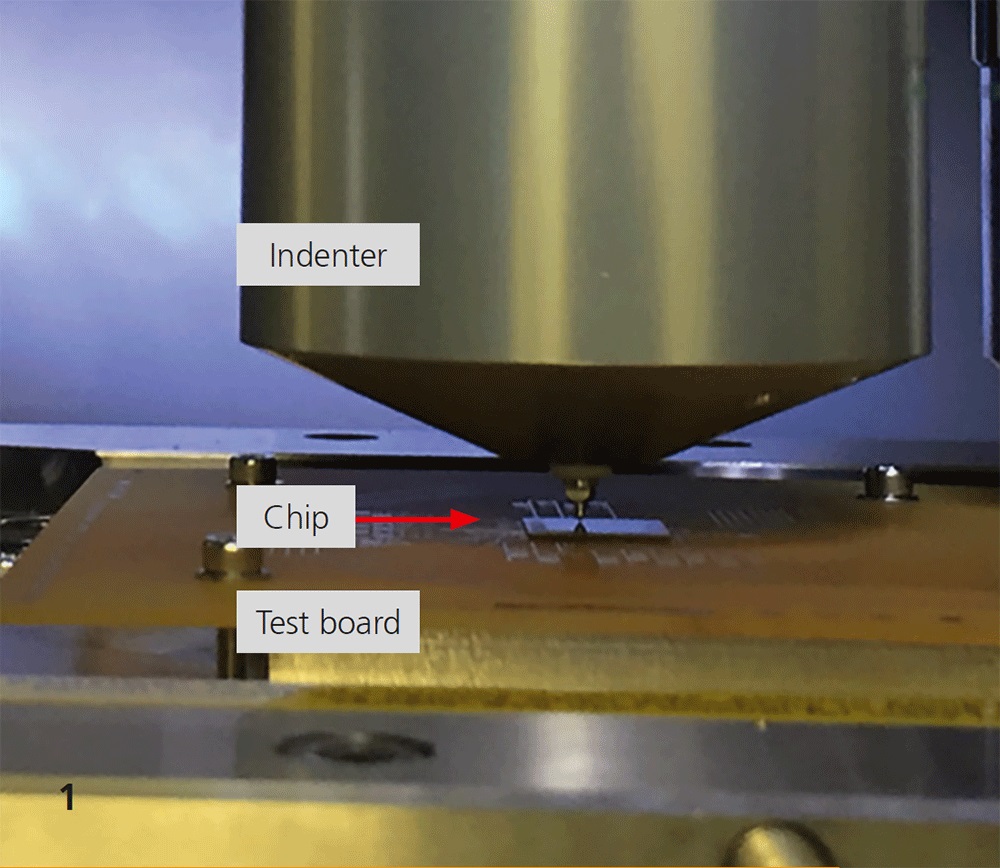
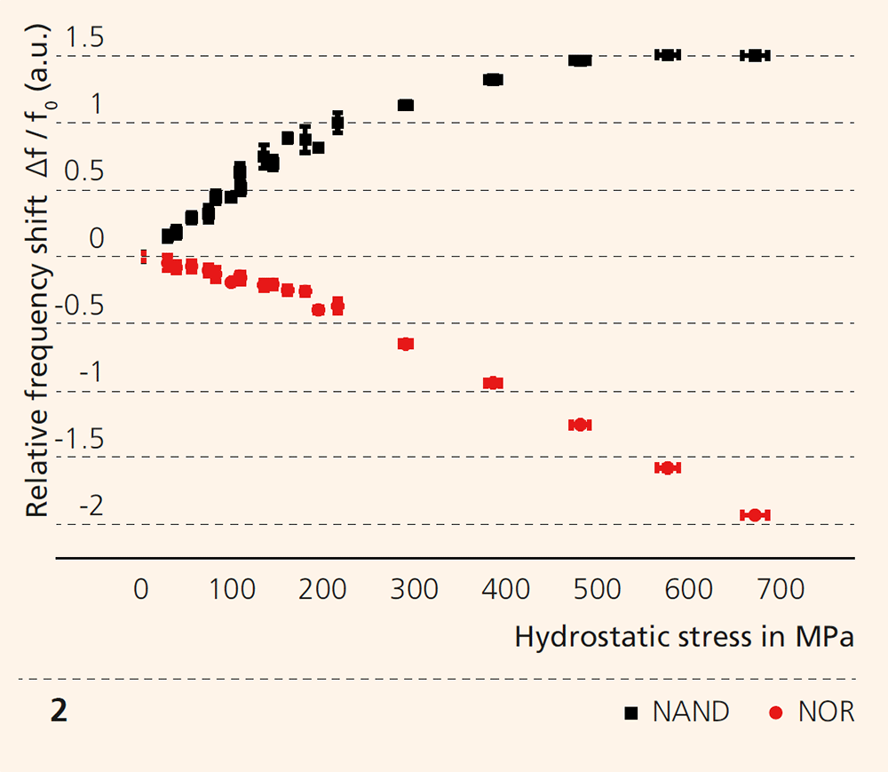
In this study, test chips with integrated stress-sensitive circuits (ring oscillators) are utilized and soldered on a board for electrical contacting. The approach allows to monitor the behavior of electrically active circuits and transistors under local mechanical load. To achieve this, the test chips are non-destructively loaded on the silicon side using an indenter with a spherical tip as depicted in Figure 1. Simultaneously, characteristic electrical signals (frequency f) of the circuits are monitored as mechanical loads continuously increase, as shown in Figure 2.
Mechanical simulations (FEM) of the full experiment are set up to compute the stresses in the transistor channels of the circuits, taking into account the experimentally applied loads, chip layouts and the selected contact geometry. The determined stress/strain is the physical root cause for the transistors’ observed parametric variations.
Two different ring oscillator structures (NAND and NOR circuits) were studied and the results observed indicate different electrical responses to the experimental loads applied, which can be explained by their specific circuit layouts. Additionally, the accuracy and resolution of the experimental approach, the working range as well as the impact of technique-related parameters were studied and improved. Based on these results, directional stress effects in transistors were also studied using cylindrical tips. Combining the indentation studies with spherical and cylindrical tips made it possible to determine quantitatively the piezoresistive coefficients of the chip technology under review, which is an excellent result with a view to implementing the process in an industrial setting. With the help of the method developed, local effects of stressed silicon and uncontrolled stresses on the components can now be estimated.
