 Fraunhofer Institute for Ceramic Technologies and Systems IKTS
Micromechanical in-situ experiments on copper interconnect structures
Current research
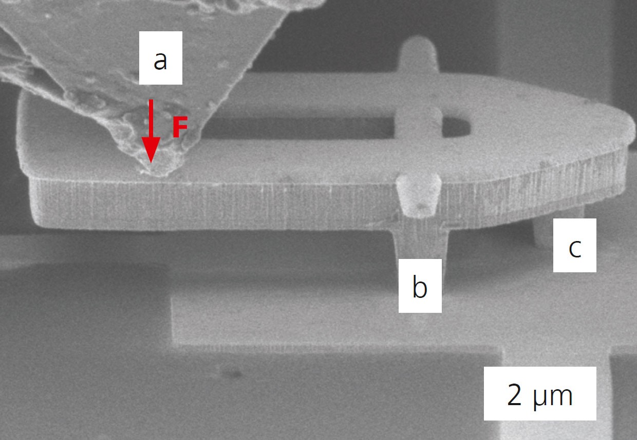
SEM image of a test structure with the indenter tip (a) in contact.
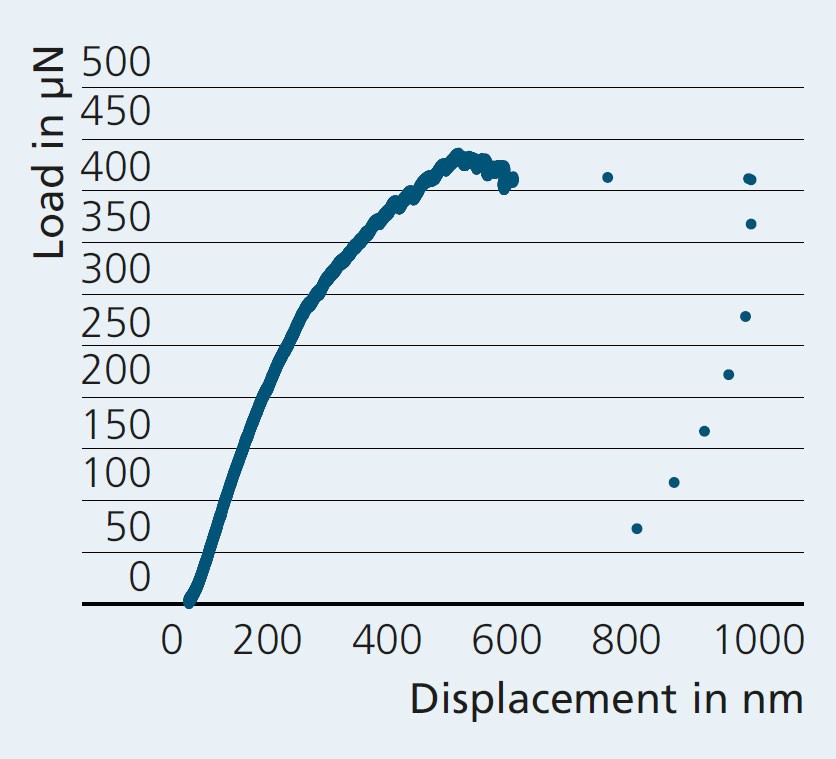
Load-displacement curve of an experiment.
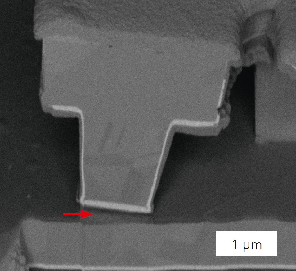
Cross-section of a tested copper via. The red arrow indicates the delaminated interface between diffusion barrier and copper.
Adhesion testing for the reliability of microelectronic devices
Adhesion testing methods for very small wiring levels in microelectronic devices [back-end- of-line (BEoL) levels], are critical for the manufacturing and reliability testing of modern microelectronic structures. However, very few measurement techniques exist, and moreover, they do not allow the inclusion of product-identical size scaling or realistic structures in the study of interface properties. Therefore, an in-situ nanoindentation-based SEM approach was developed at Fraunhofer IKTS. It enables investigating product-like copper via structures that are just a few micrometers in size – and thus for the first time analyzing the interfaces of individual industrially manufactured vias.
Optimized micromechanical experiments
For the new approach, a nanoindentation system is installed inside the vacuum chamber of a scanning electron microscope (SEM). This makes it possible to accurately position the wedge-shaped indenter tip on the micron-sized test structures. The test structures are designed as cantilevers (top image). For the investigations, a load is applied to the cantilever at its freestanding side using the indenter tip (a); the force is then converted into a tensile force through a hinge via (b). This hinge via then engages, across the rear via (c), on the via underside of the interface under investigation. This causes the interface under the rear via to delaminate. In the recorded load-displacement data, the delamination event is indicated by a severe load drop (middle figure).
High variability of test structures
The test structures are prepared using the copper damascene process, which is widely applied in the industrial manufacturing of BEoL structures and generates test structures with a large variety of designs. This allows for other experimental designs, such as the testing of interfaces for different loading modes. Also, the process generates a high number of identical test structures to ensure that measured data are statistically well reproducible.
By slightly altering the manufacturing sequence, it is also possible to create different interfaces on the test via. Important interfaces with regard to the reliability of BEoL structures exist, for example, between copper, silicon nitride, diffusion barriers, and silicon oxide. The bottom image exemplifies the cross-section of a delaminated interface between copper and a diffusion barrier (indicated by a red arrow).
The interfacial delamination made quantitatively accessible by this method forms the basis for FEM simulations which support reliability testing and help improve the design of interconnect structures in microelectronics.