
Microelectronic devices for automotive applications need a stringent reliability assessment due to a high-stress environment and expected long lifetimes. Additionally, they are becoming increasingly miniaturized thanks to advanced technologies.
Fraunhofer IKTS has investigated the reliability of leading-edge 28 nm high-k metal gate CMOS SRAM circuits (GLOBALFOUNDRIES Dresden) with applied mechanical loads. For detailed investigations, we developed a new three-in-one test method combining a mechanical process based on nanoindentation, an electrical test setup, and FEM simulations of mechanically induced stresses at the transistor level.
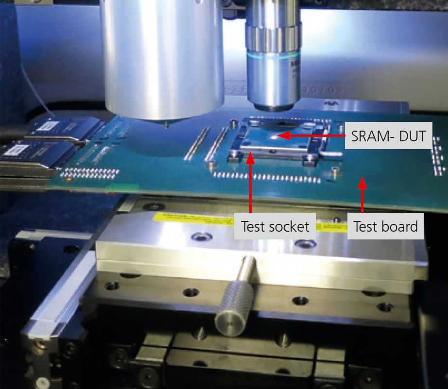
This approach makes it possible to examine chip-package-interaction (CPI) and chip-board-interaction (CBI) for novel SRAM devices in operation and to detect potential failures of the architecture. The chips were assembled on a flip chip substrate without a lid and the silicon was thinned down to a minimum of 16 μm at the back side. To enable electrical in-situ measurements, the chip was connected to a socket before, during, and after the indentation with forces of various magnitudes. The experimental setup with the used SRAM chips is shown in Figure 1.
The first step – the spherical, elastic nanoindentation – is performed on several spots at the backside of the chip. This is followed by the electrical measurement, which incorporates a read-fault procedure and a bit-cell-fault calibration procedure to determine eventual bit flips with applied load.
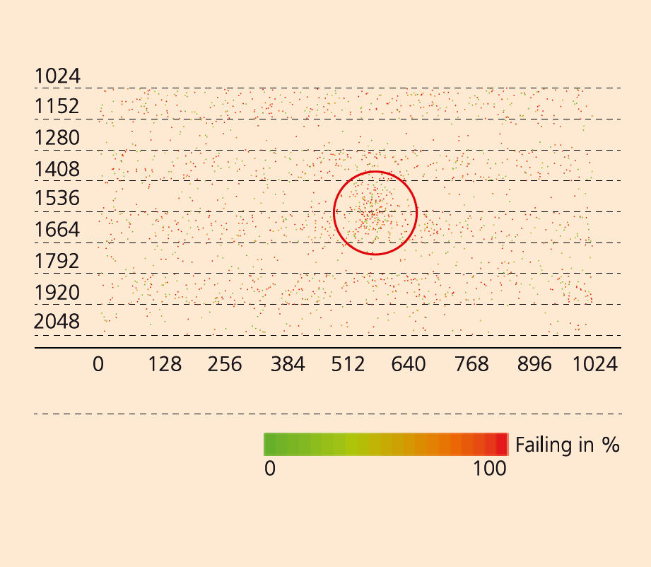
For the read-fault procedure, a chessboard pattern is written in, with the writing step taking place with an undervoltage at the bit flip threshold. The bit flips are detected in the subsequent reading step with target conditions. After 50 repetitions, the error frequency is correlated with the load. Figure 2 shows a bit cell fault matrix with additional background noise for an applied load of 1.3 N. Loading leads to a significant 40 % radial increase of the bit cell fault probability at the indentation area (red circle). The process is fully reversible, meaning that the fault disappears upon unloading. As a last step, the results thus obtained are compared with FEM simulations using the SRAM layout and the semiconductor stack parameters to predict optimal indentation points and stress/strain fields at the indented area. Furthermore, the described test approach is suitable for estimating mechanical stress on active transistor regions and can be used for design optimization on the chip, package and board levels. We plan to conduct further investigations of new leading-edge technologies.
This work was a collaboration of Volkswagen AG Wolfsburg, GLOBALFOUNDRIES Dresden, Fraunhofer IKTS, and Fraunhofer IIS-EAS.