 Fraunhofer Institute for Ceramic Technologies and Systems IKTS
Determining microscopically adhesive and cohesive material behavior
Current research

Patented in-situ four-point bending tool.
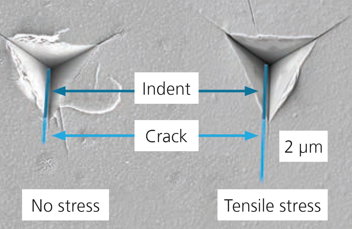
Nanoindentation experiments at non-strained (left) and tensile-strained silicon dioxide thin films (right) leading to big differences in the ratios between indentation corner length (IL) to crack length (CL).
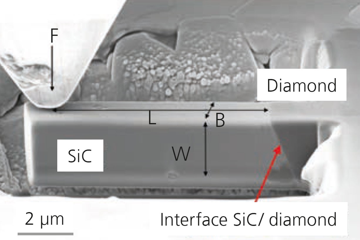
Focused-ion-beam-prepared micro bending cantilever for testing the SiC to diamond interface in the microstructure of a SiC-bonded diamond material [1].
The macroscopic behavior of heterogeneous materials and components is mainly determined by micromechanical properties. This is especially true for microscopically structured systems, such as for instance thin-film systems. Therefore, characterization on the microscopic level is essential, besides macroscopic characterization, to understand the behavior of materials and systems. Only this understanding enables the target-oriented future development of structural and functional ceramics, microelectronics, as well as micromechanical systems.
When it comes to micromechanical characterization, Fraunhofer IKTS has vast amounts of experience and equipment, e.g. in measuring local elastic properties, mechanical stress at room and elevated temperatures, stress-strain curves, local adhesion of interfaces and grain boundaries of structural and functional materials, as well as in determining the cohesive behavior of thin films.
Microscopically cohesive failure of silicon dioxide thin films
Thin films made of silicon dioxide (SiO2) serve as insulating layers in microelectronics and must be highly stable against cohesive fracture propagation, which requires quantitative determination of cohesive properties of the thin-film material. However, thin-film systems are not suitable for macroscopic characterization methods, due to their dimensions. There-fore, nanoindentation (NI)-induced fracture propagation is used. To separate the measured cohesive material parameters from the superimposed residual stresses of the films, the NI fracture experiments must be conducted at several different stress states of the film. This is done with the in-situ four-point-bending system (top image), developed and patented at Fraunhofer IKTS. With application of this system, the stress in the SiO2 film can be adjusted to different levels, at which NI fracture tests can be readily conducted. The different stress levels lead to considerable differences in fracture propagation (second figure). With this information, a fracture toughness can be derived that is free from the effects of residual stresses.
Stability of diamond – silicon carbide interfaces
The firm inclusion of diamond particles in silicon carbide (SiC)-embedded diamond materials is essential for the immensely high wear resistance and hardness of these materials. The stability at the interfaces between diamond particles and SiC matrix can be investigated through microcantilever beam tests in the vacuum chamber of a scanning electron microscope and subsequent inspection of the fracture surface. The microcantilevers can be prepared with such precision, using a focused ion beam (FIB), that the interface of interest is located at the fixed end of the cantilever beam (third figure). Thereby, the cantilever is stressed with a high-resolution indenter, acquiring load-displacement curves (bottom figure). With this method, it was possible, for the first time, to confirm the firm embedment of the diamond particles via the epitaxial growth of the SiC matrix during fabrication. [1]
Literature
[1] Ast et. al (2021), doi: 10.1016/j.oceram.2021.100176) .
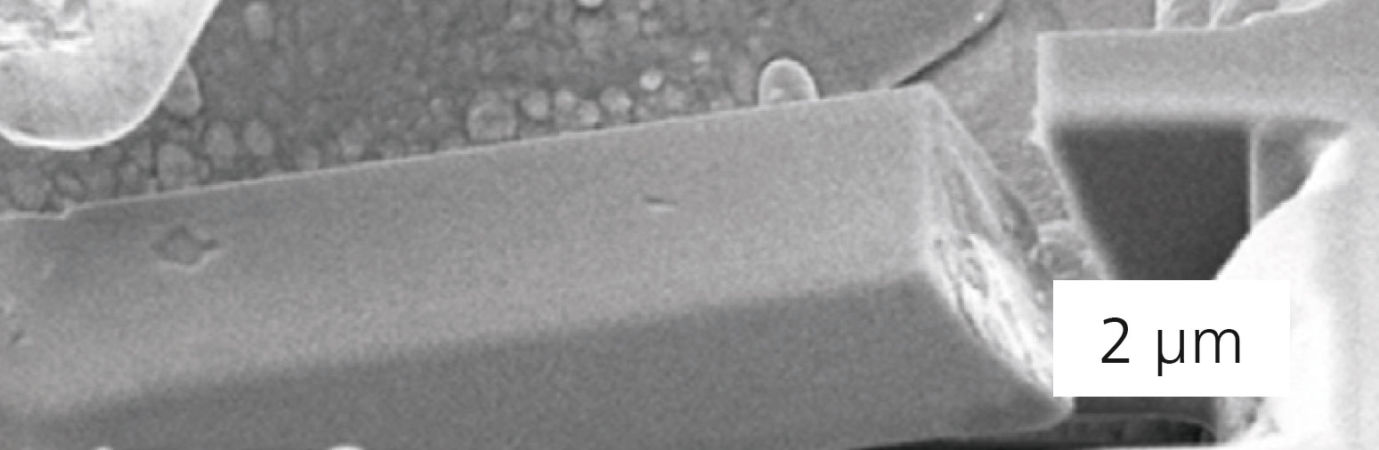
In-situ micro-bending test in the scanning electron microscope showing adhesive interface failure between SiC and diamond [1].