 Fraunhofer Institute for Ceramic Technologies and Systems IKTS
New approaches for in-situ analytics in microelectronics
Current research
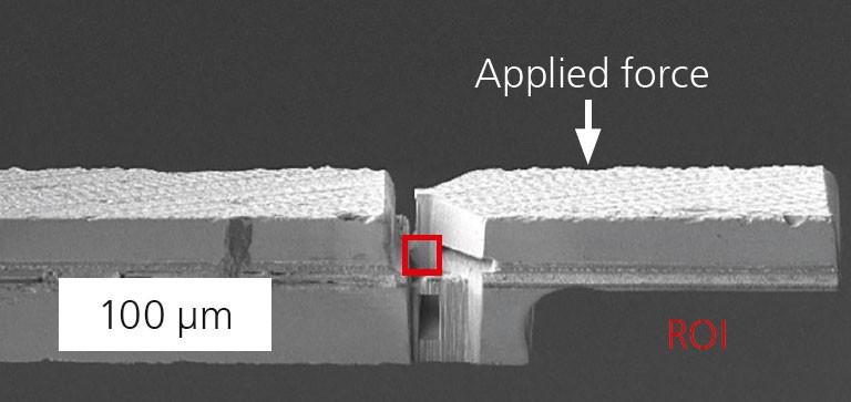
Push-to-pull sample for in-situ nanoXCT nano-mechanical testing of BEoL structures
(prepared using plasma-FIB).
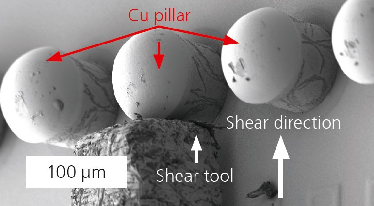
In-situ SEM shear experiment setup.
3D nano-X-ray tomography of μ-cracks in wiring stacks on microchips
On-chip interconnect stacks (Back-End of Line BEoL) of microelectronic technologies consist of increasingly fine structures of various materials like copper or nanoporous dieletrics. This leads to higher demands on their mechanical stability and therefore their reliability under various loads, such as chip package interaction (CPI). New methods for the study of these fine structures are X-ray microscopy and based on that 3D nano-X-ray tomography (nanoXCT). The latter with its resolution of 50 nm is perfectly suitable for in-situ nanoXCT microcrack experiments for the analysis of mechanically weak spots in the BEoL.
Image 1 shows a complex lever-based push-to-pull sample geometry manufactured by plasmaFIB, which introduces a crack in tensilemode into the region of interest (ROI) in the BEoL. During the micromechanical experiment,the crack propagation in the ROI can be observed in high resolution in 2D and 3D and understood. On the basis of such complex micromechanical in-situ nanoXCT workflows, more mechanically stable microchip technologies for demanding applications like automotive electronics can emerge in the future.
Crack identification in Back-End of Line (BEoL) stacks
In the industry, the investigation of the stability of solder bumps and copper pillar geometriesis already established. However, there is no comparable standard for the underlying crack-prone BEoL stacks. At Fraunhofer IKTS, a method was adapted to observe crack initiation and propagation in copper pillar/BEoL systems.
First, external forces are applied to the copper pillar to evaluate the mechanical stability of BEoL stacks. This is done by shear loading with an in-situ (image 2) or ex-situ nanoindenter system (image 3a). An acoustic emission (AE) detection sensor, attached to the sample, identifies and measures acoustic waves indicative of damage during the shear experiment (figure). The much higher temporal resolution of the AE measurements compared to the piezo sensors of the indenter allows a more accurate insight into the damage process. Subsequently, the resulting damages are further investigated with nanoanalytics methods, such as nano-X-ray computed tomography (nano-XCT, image 3b, c) and scanning electron microscopy (SEM, image 2).
The results allow for a better understanding ofthe origin and propagation of damage in the BEoL stack. The nanoXCT damage analysis of the example depicted in the images shows that the BEoL stack not only delaminates locally, but that cracks can also propagate horizontally along the layers, which are not detectable with other optical measurement methods. Additional in-situ shear tests on copper pillarsin the nanoXCT and SEM offer a more precise insight into crack formation.
In the future, these investigations will complement the analysis of BEoL structures and characterize crack propagation more precisely. This will bring decisive advantages for reliability assessment.
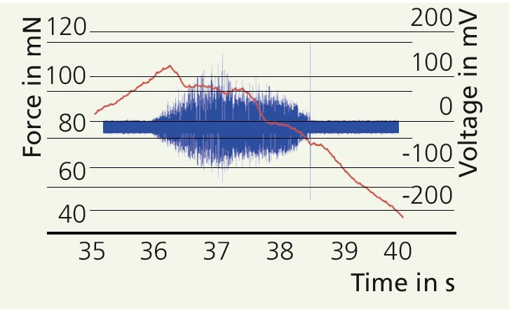
Force progression curve (red) with piezo voltage of AE signal
(blue) of SnAg cap shear and image of resulting damage.
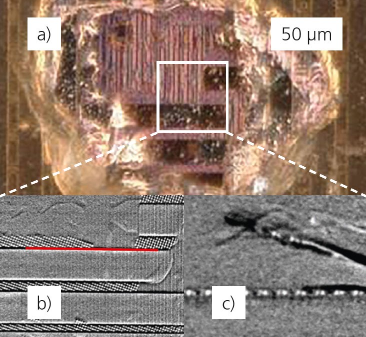
nanoXCT damage analysis: Optical microscopy overview image (a), details with sub-surface crack location (b), and virtual cross section with side view of the crack (c).