Application examples

Topic

The development activities of the Thick-Film Technology group with its focus on functional printing over the course of the years have resulted in a comprehensive portfolio of functional special pastes and inks for applications in composite assemblies and components, as well as sensors in electronics, power electronics, microsystem technology, energy and environmental technology.

The following examples demonstrate current development topics, e.g. from the fields of additive manufacturing and 3D printing. In addition to special pastes and inks for the surface functionalization of 3D components manufactured with additive methods, we also develop pastes for the additive 3D printing of ceramic components. Printed electronics and the development of electrochemical pH sensors for water analysis are other fields we work in.
Heavy-metal ion sensor


Within the framework of the ZIM project “SSB Chalk” (KF2087359KM4), which is sponsored by the German Federal Ministry for Economic Affairs and Energy, Fraunhofer IKTS develops an efficient process for manufacturing miniaturized thick-film-based heavy-metal ion selective electrodes (ISE), in cooperation with partners from the private and research sectors. Such sensors are used for water analysis applications (environment and process water monitoring).

One particular challenge of this project is to develop materials and processes for the deposition of chalcogenide glass thick-film membranes on a ceramic substrate. The advantages of the thick-film-based heavy-metal ion sensor are that it is mechanically robust, offers a high chemical resistance and density, and that it can be manufactured cost-efficiently in large quantities.

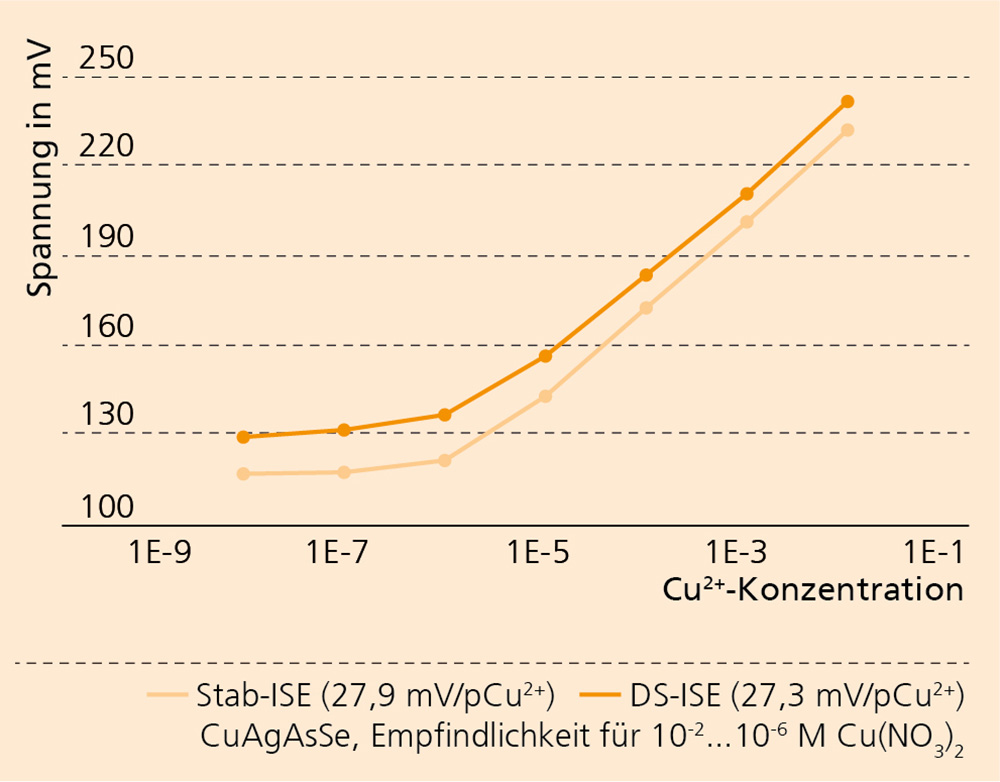
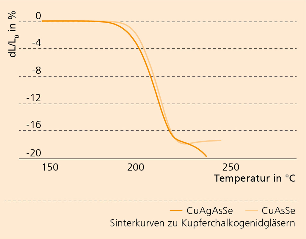
We have developed thick-film-based potentiometric ISEs based on the copper chalcogenide glasses CuAgAsSe and CuAsSe, in order to detect copper in aqueous solutions. According to the thermochemical, crystallization and sintering behavior of the glasses, the thick-film pastes made from the glasses were processed in such a way that thin glass membranes were deposited on ceramics which are copper ion-sensitive. The sensitivity of a CuAgAsSe thick-film electrode is within the measuring range of 10-2 M to 10-6 M Cu(NO3)2 solution at 27.3 mV/pCu2+. This value corresponds to the Nernst behavior for divalent ions and correlates well with the sensitivity of the bulk material.

© Fraunhofer IKTS
Empfindlichkeit der CuAgAsSe-Chalkogenidglaselektroden.
© Fraunhofer IKTS
Sinterkurven der Kupferchalkogenidgläser.
© Fraunhofer IKTS
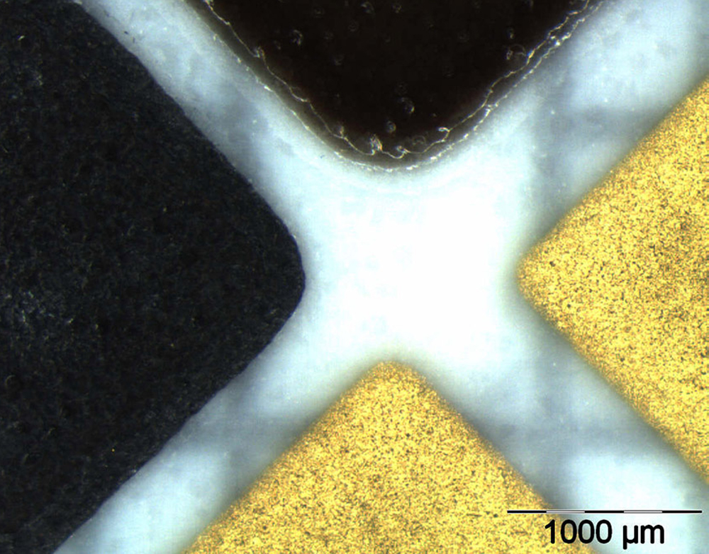
Microscopic image of an ion-selective electrode.

Electrochemical sensors for water analysis: Mini pH sensor


The potential offered by ceramic multilayer technology with regard to materials and technology can be used for the development of electrochemical sensors, in particular when it comes to measuring pH values. The strengths of ceramic multilayer sensors are their high integration rate, which stems from the 3D structure, their mechanical robustness, high chemical resistance and density, and therefore their low susceptibility to disturbing factors. Using ceramic multilayer technology, we have manufactured a miniaturized all-solid-state pH sensor (see downloads), which offers a very good measuring performance with regard to sensitivity, response time and potential stability.


Sensor properties


  • pH measuring range: 1 to 9 pH
  • pH sensitivity NERNST behavior
  • Response time t90 ≤ 1 s
  • Temperature range: 25 to 45 °C
Potentiometrischer Mini-pH-Sensor in HTCC-Technologie.
© Fraunhofer IKTS
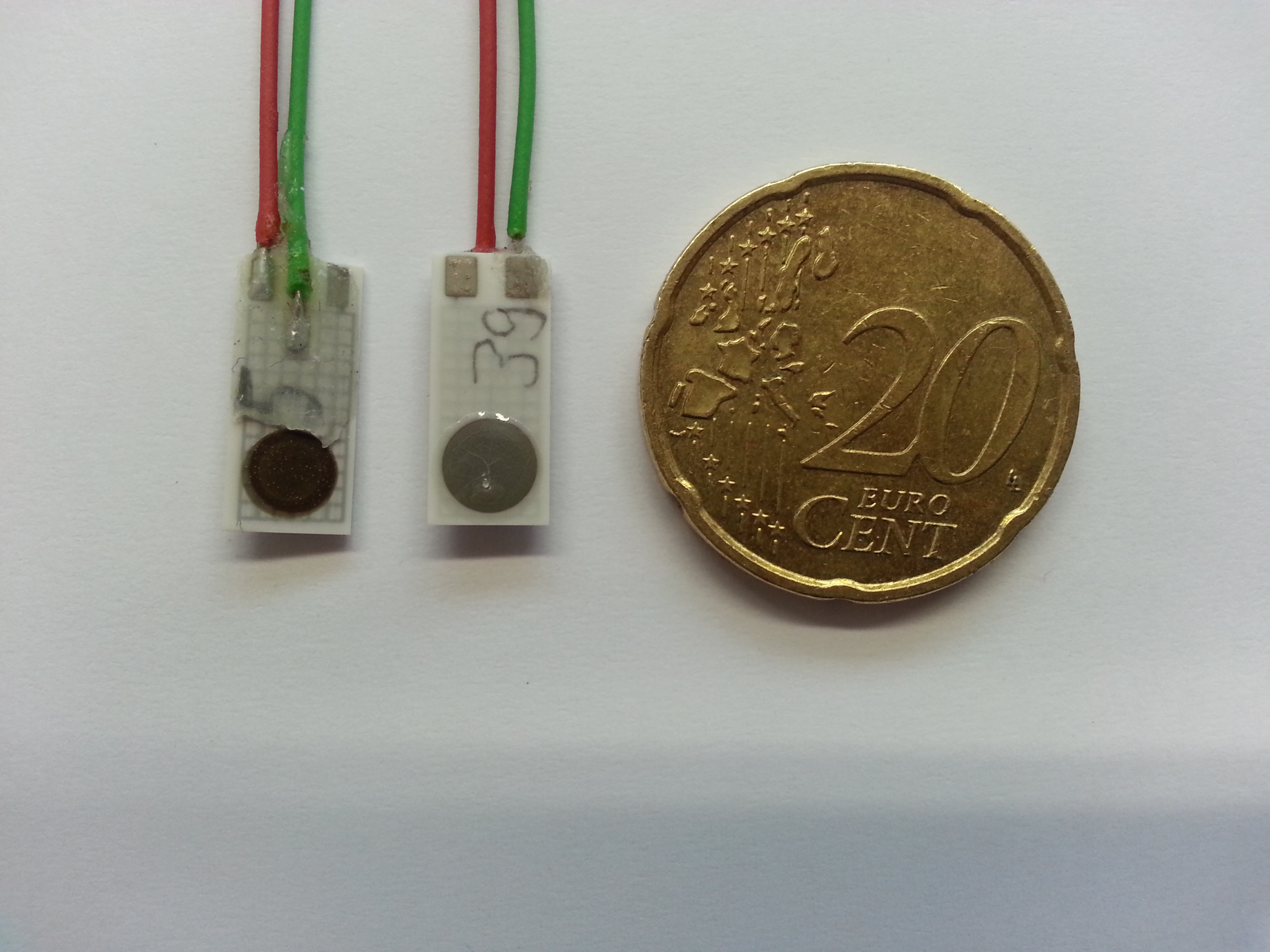
Potentiometric mini pH sensor with HTCC technology.
© Fraunhofer IKTS
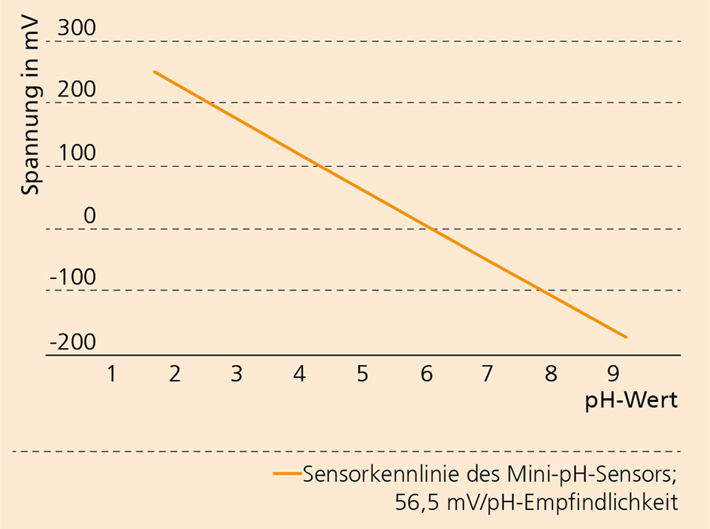
Sensorkennlinie eines Mini-pH-Sensors.
© Fraunhofer IKTS
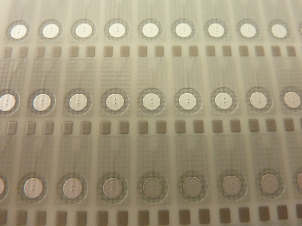
Manufacture of the mini pH sensors with multiple uses.

Functionalization of ceramic 3D components

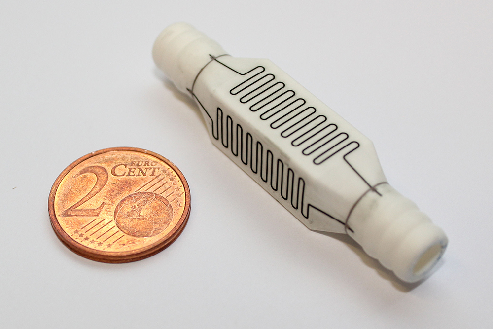
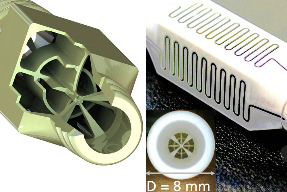
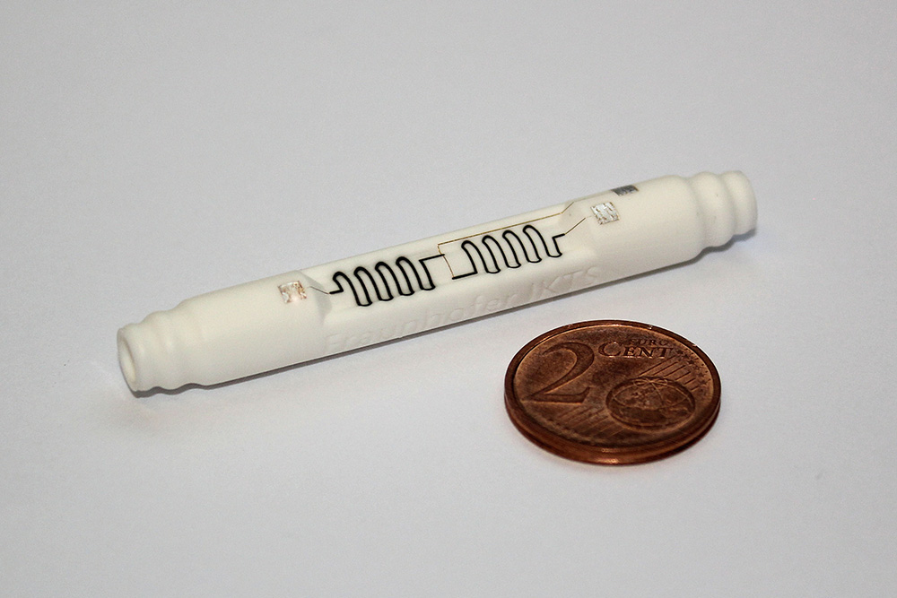
Current 3D printing technologies enable highly complex ceramic components which would have been impossible to manufacture before. The Thick-Film Technology group with its focus on functional printing develops customized pastes and inks for 3D printing (dispensing, dispense jet, aerosol jet), e.g. in order to deposit electrodes, sensors or heating elements on the surfaces of ceramic components which were manufactured in additive processes. Printing can take place on tubular substrates, free-form spherical shapes, as well as in cavities or canals. Such ceramic products with intelligently functionalized 3D components (see Downloads) are resistant even to harsh environmental conditions.

© Fraunhofer IKTS
Fluid mixer with heating meander for tempering (max. > 130 °C).
© Fraunhofer IKTS
Fluid mixer with heating meander for tempering, design and implementation of the 3D component.
© Fraunhofer IKTS
Printed membrane of a ceramic flow sensor (wall thickness dW < 0.3 mm).

Low-temperature pastes for printed electronics

Printed electronics as a field of application for pastes poses requirements which conventional thick-film technology was not able to meet until now. In contrast to conventional thick-film pastes, printed pastes have to be formed at temperatures below 300 °C in order to retain functional layers. For this purpose, we at Fraunhofer IKTS have developed low-temperature pastes.

The polymer is the main component of such pastes for printed electronics. It produces the adhesiveness on the substrate and fixates the particles in the functional phase. The suitable polymers are selected according to curing temperature, the operation conditions of the resulting functional layer with regard to temperature, moisture and substrate quality.

Depending on the layer deposition technology (mask-based or digital), and the required curing profile, appropriate solvents or solvent combinations are used. They are used to adjust the required rheology of the functional suspension. Depending on the field of application, metal powders can be used to produce conductor layers, while ceramic powders can be used to produce insulating layers, and carbon modifications for resistor layers. In contrast to conventional thick film pastes, thermal curing is not always followed by a sintering of the functional powders. The properties are achieved either by percolating the particles introduced in the final layered composite, or, where nanoparticles are used, by producing sintering necks. This requires high volume shares and the optimal dispersing of the functional phase, in particular for conductor pastes.

© Fraunhofer IKTS
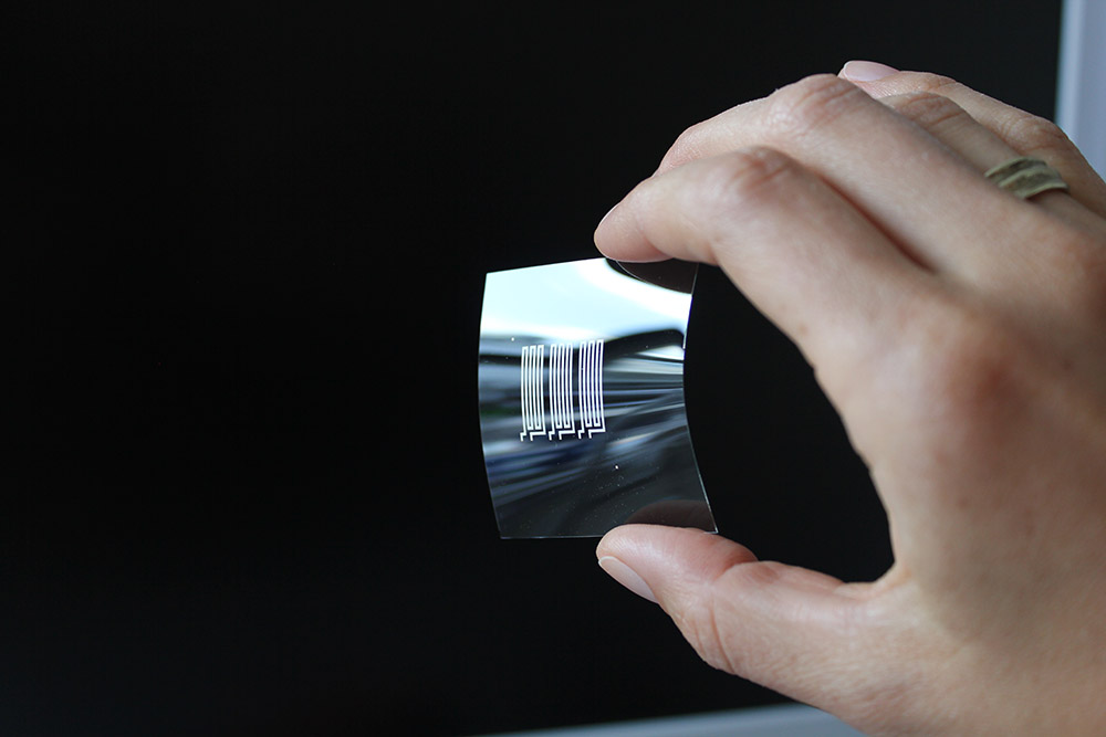
Thin glass with polymer conductor paste.
© Fraunhofer IKTS
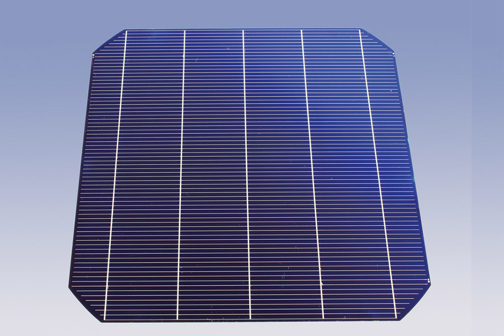
MWT+ solar cell with conductor paste on silver-polymer basis.
© Fraunhofer IKTS
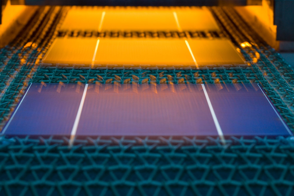
Metallization technologies for silicon-based solar cells. Firing of the metallization paste.