Photoimageable pastes for high-frequency applications
Current research


Photoimageable thick-film pastes – the new path for high-speed internet?
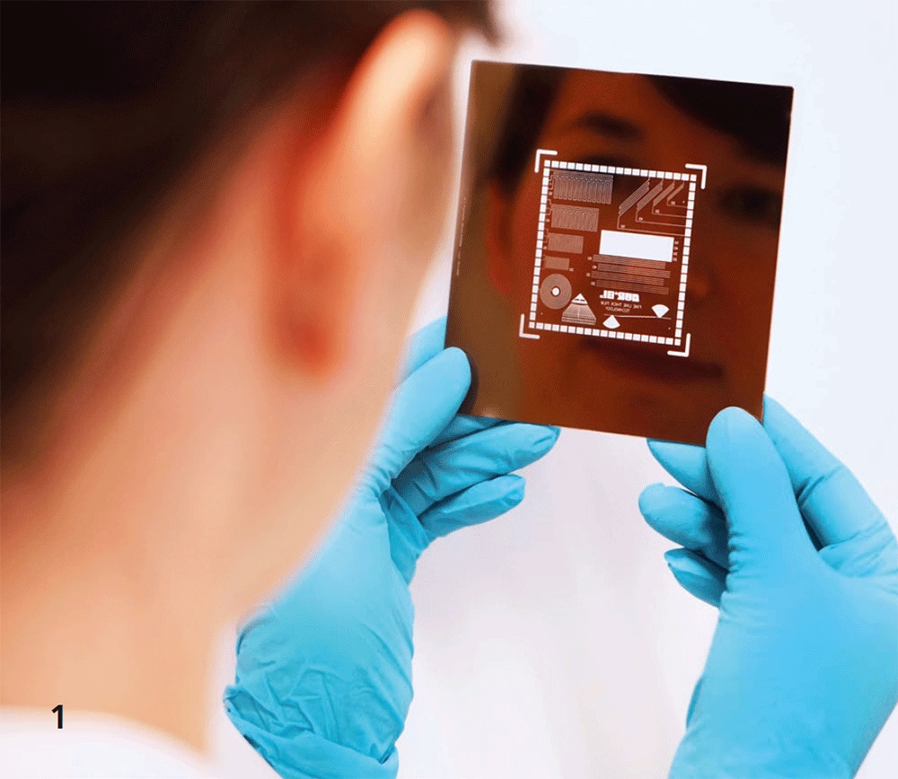
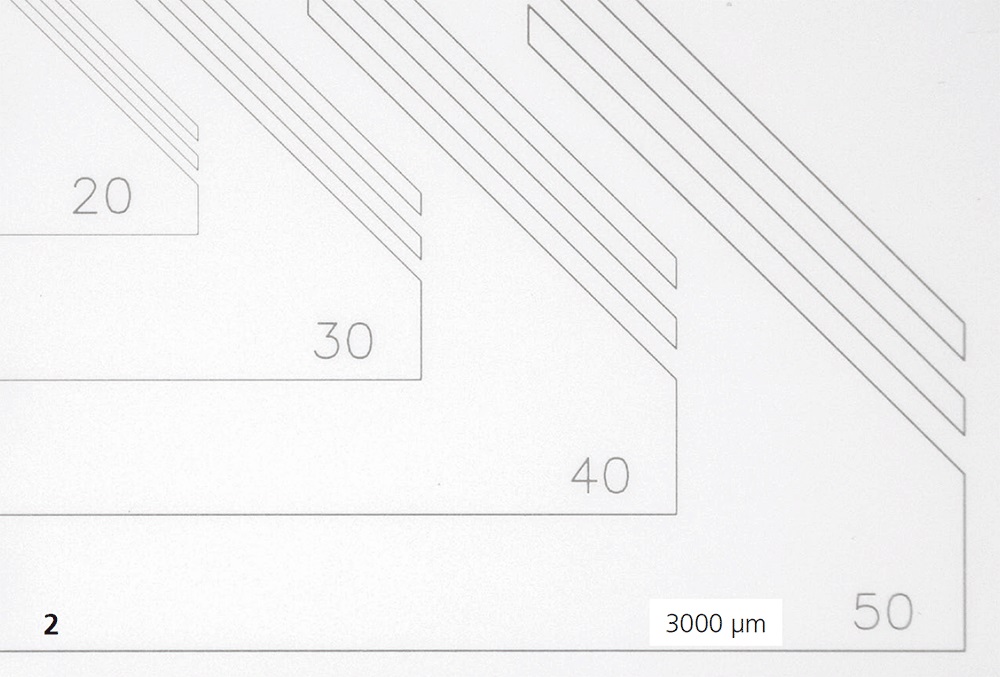
The next generation of mobile internet and mobile communication is here: the Fifth Generation – 5G for short. For transmitting and receiving signals, this technology requires electronics and associated antennas with significantly finer structures than before. Initially, it will operate at 3.6 GHz and later at even higher frequencies. In terms of miniaturization, the thick-film technology currently used has reached its limits: A resolution of around 50 micrometers (μm) is the limit today – at least regarding industrial implementation. This means the individual electrical structures, such as conductors, are at least 50 μm wide. The 5G standard, however, requires circuitry as fine as 20 μm and smaller. One option to generate such structural dimensions industrially by means of thick-film technology is called PI technology (PI = photoimageable). Fraunhofer IKTS has developed a new generation of thick-film pastes which enable photolithographic structuring. With these new PI pastes, extremely high-resolution thick-film structures with a 20 μm sintered line width and 20 μm line spacing can be produced. As in the standard thick-film process, screen printing technology is used as the deposition process. PI technology adds only two simple steps to this process: In a first step, the printed and dried paste is exposed to UV light using a photo mask or a laser (laser direct imaging, LDI). The exposed paste structures are cured and the unexposed structures are removed in a second step. Immediately after the wet chemical development, the samples are sintered in a standard thick-film regime to produce the final properties of the functional layer. The two additional steps require only between 5 and 20 seconds each and can be easily integrated into the production process line. It is also possible to work in a normal laboratory environment without the UV-protective measures necessary in other photolithographic processes.
Tailor-made thick-film pastes are required for the PI technology to work. At the present time of development, Fraunhofer IKTS has developed PI paste systems based on silver and gold, which can be used for both sintered aluminum oxide and non-sintered LTCC (low temperature co-fired ceramics). For silver, sheet resistivities of less than 3.5 mohms/sq can be achieved, for gold less than 6 mohms/sq. Current research includes adapting PI paste systems to a variety of ceramic systems, as well as developing other paste materials, such as platinum, silver/palladium, dielectric and resistor pastes. This offers a promising paste portfolio, with which components can be produced that achieve a significantly better RF performance than previously possible, at higher frequencies. The pastes can be used directly in mass and industrial processes with low investment costs and only slightly higher production times.