Packaging

Topic

systemintegration1
SMD pick and place
aufbau-und-verbindung
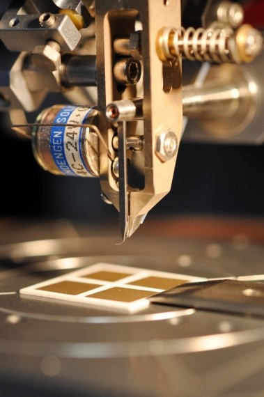
SMD placing

The advantages of ceramic wiring substrates and sensors exist in the favorable mechanical properties, as well as in the excellent thermal conductivity of the substrate materials and the very low-cost, matched to silicon thermal expansion coefficient. In addition to the assembly of discrete components, these parameters allow the processing of unhoused semiconductor devices.

In this case, the electrical connecting contact between the semiconductor and ceramic wiring substrate by wire bonding or soldering is performed. Since the ceramic wiring substrates are typically used in the field of power electronics, the use of higher wire diameters and special wire materials is dominant.


Services offered


  • Dimensioning, design and realization of prototypes for thick-film circuits
  • Development and optimization of packaging solutions for thick-film based modules
  • Technology optimization of assembly processes and materials selection
    • Soldering
    • Adherence
    • Wire bonding
  • Thermal aging
  • Failure analysis


Technical equipment


  • Screen printer EKRA
  • Continuous furnace Centrotherm
  • Wire bonder (R & K Delvotec)
  • Manual placement machine (essemtec AG EXP SA)
  • Pull/shear tester DAGE 4000
  • Batch soldering furnace Focus 350
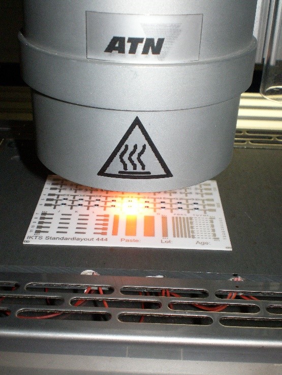
  • Selective soldering station ATN
Light soldering head.

Selective Soldering


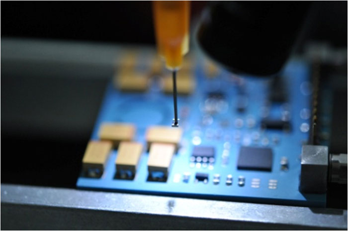
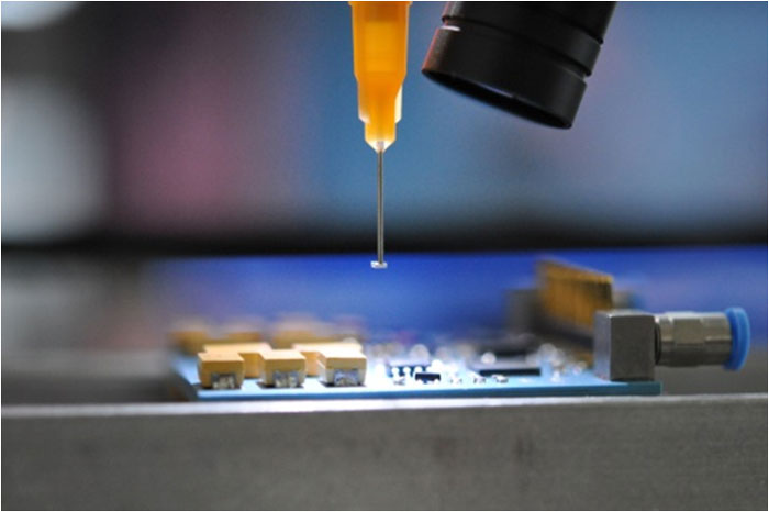
In the field of soldering, the work of the group is focused on selective soldering. For this, special equipment for the spatially resolved reflow soldering based on light, laser and the induction soldering is available.

Based on the applied processes, soldering temperatures up to 600 ° C can be achieved. This fact allows the use of high-melting solder alloys in air atmosphere.

  Laser soldering Light soldering Inductor soldering
Power / W 32 250 2600
Focus diameter / mm < 1,5 < 3 < 6
Work distance / mm 70 - 80 30 - 50 < 1
work paramteter 908 nm 500 - 1500 nm 0,5 - 1,0 MHz
Temperature range / °C < 450 < 450 < 850
Soldering time / s < 3 < 5 < 3
Dependence surface surface geometry
Application example Interconnection of cell bus bars Interconnection of cell bus bars Interconnection of cell strings
difficult-to-reach soldering joints drying of adhesives interconnection of engine conrtol units (automotive)
Advantage contact soldering small soldering joints surface heating absolute constant heating
short process time, contactless, low maintenance


The selective soldering methods are also advantageous in the packaging of temperature-sensitive components.

Wire Bonding


In the area of the wire bonding, the following  technologies  are available:


Process
Wire Material Remarks
Thin Wire Ball-Wedge Bonding Au (Typical Diameter 25 µm) Special wires on request
Thin Wire Wedge-Wedge Bonding Al (Typical Diameter 25 µm)  
Thick Wire Wedge-Wedge Bonding Al, Cu (Diameter up to 500mm) Special wires on request
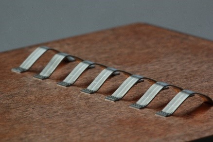
Ribbon bonding Al (200 µm x 2000 µm)  


Thin wire bonding is mainly used for contacting high-temperature suitable sensor elements. For applications in the field of power electronics, it is necessary to use large conducting path cross-sections. In this respect, the use of thick-wire or ribbon connections is dominant

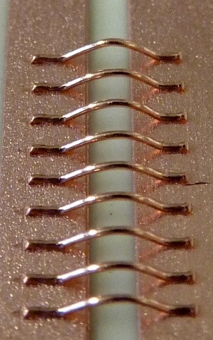
Copper thick wire bonds on DCB substrate.
Alumina ribbon bonds on AMB substrate.