 Fraunhofer Institute for Ceramic Technologies and Systems IKTS
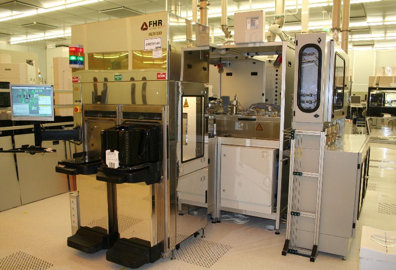
According to the development objectives of the microelectronic industry the density of devices on the semiconductor chips increases and the device dimensions shrink. This is also valid for storage capacitors in DRAM (dynamic random access memory) which is the main memory of the computer. One method for achieving high capacities in future generations of storage cells is the development of so-called high-k materials which means materials with high dielectric constants. These new materials will be deposited by ALD (atomic layer deposition). ALD allows a well-defined deposition of atomic layer by atomic layer with a high homogeneity. Fraunhofer IKTS is involved in the search for new high-k materials using ALD and sol-gel techniques as well as in the technological research for ALD processes.
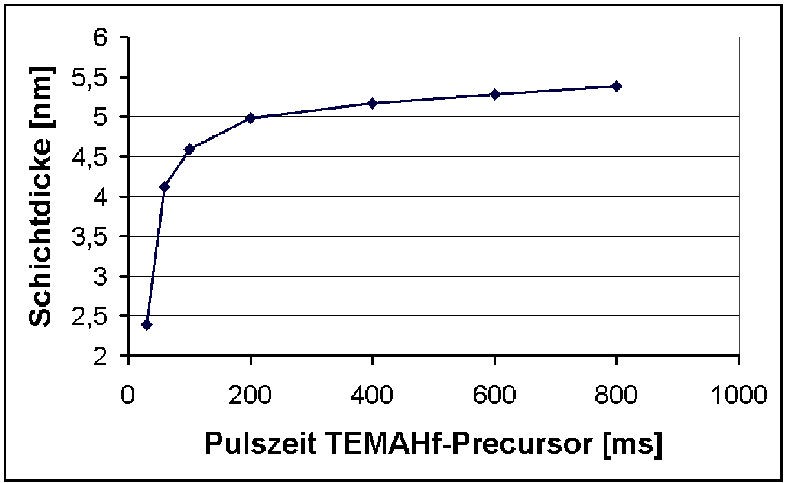
An ALD tool for the deposition on 300 mm silicon wafers was installed in the clean room of Fraunhofer Center Nanoelectronic Technology (CNT) funded by a common investment of IKTS and CNT. The tool is equipped with two process chambers allowing the preparation of different dielectrics. ZrO2 and HfO2 based materials are in the focus. Both systems offer a high application potential because of the possibility to achieve high dielectric constants up to εr = 40 in dependence on the crystal structure. The central figure shows the examination result of the ALD process window related to the HfO2 deposition with TEMAHf. During the ALD process the precursors are fed sequentially into the chamber. Between each precursor pulse the chamber is purged with inert gas. Therefore, the pulse time of the hafnium precursor is an important process parameter. It can be concluded that a pulse time > 250 ms is required for the deposition process. Only under these conditions a complete atomic layer of HfO2 is developed. The film thickness depicted in the figure is the result of an ALD process after 50 cycles. The sol-gel method is also applied for evaluating new dielectrics. The lower figure shows a 20 nm thick ceramic film between two platinum electrodes prepared by sol-gel technique.
Products and services offered
- Manufacturing of nanoscale ceramic materials with layer thicknesses between 4 nm and 100 nm
- Layer development and coating prototypes
- Complex layer characterization
Technical equipment
- ALD Cluster ALD 300 (FHR Anlagenbau)
- 4“ Spin Coater (Convac)
Examples and references
- Preparation of oxide coatings made of Al2O3, HfO2, ZrO2 using ALD
- Laminates of different materials, e.g. laminates of oxides
- Development and manufacturing of perovskite coatings with very high dielectric constants