

ALD Lab Saxony
Atomic layer deposition (ALD) is currently the fastest growing thin-film deposition technology, boasting an annual equipment and precursor market volume in excess of USD two billion. Over the last decade Dresden has become a hotbed for ALD. In spring 2016, ALD Lab Saxony was founded as a division of Cool Silicon e. V. within Silicon Saxony e. V. It combines several universities and research institutes from Saxony and forms the largest German ALD cluster. Fraunhofer IKTS is one of the founding members of ALD Lab Saxony. Members from ALD Lab Saxony took part in the ALD conference 2016 in Dublin, Ireland, as chairs and attendees, presenting a total of 18 contributions (posters and talks).
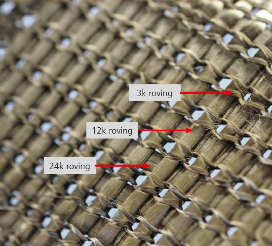
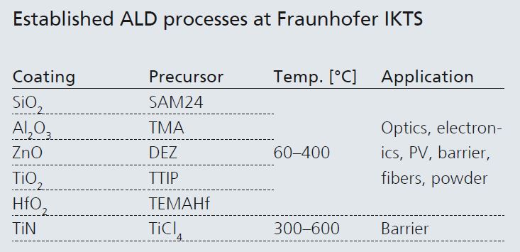
CVD and ALD deposition techniques present diverse possibilities for accommodating the heightened interest in thin and ultrathin conformal coatings for numerous applications seen today. Fraunhofer IKTS possesses capabilities for coating fiber materials and textile preforms with protective layers by ALD and CVD. Besides offering barrier and protective layers, Fraunhofer IKTS has a strong focus on ALD applications in the field of energy harvesting and storage systems. Ultrathin conformal coatings made of advanced multicomponent layers and nanolaminates are offered for backside passivation in photovoltaic devices and as lifetime enhancement layers in Li-ion batteries. Coating of powders is performed by ALD and CVD with a rotating drum technology.
Core competencies in ALD processing at Fraunhofer IKTS
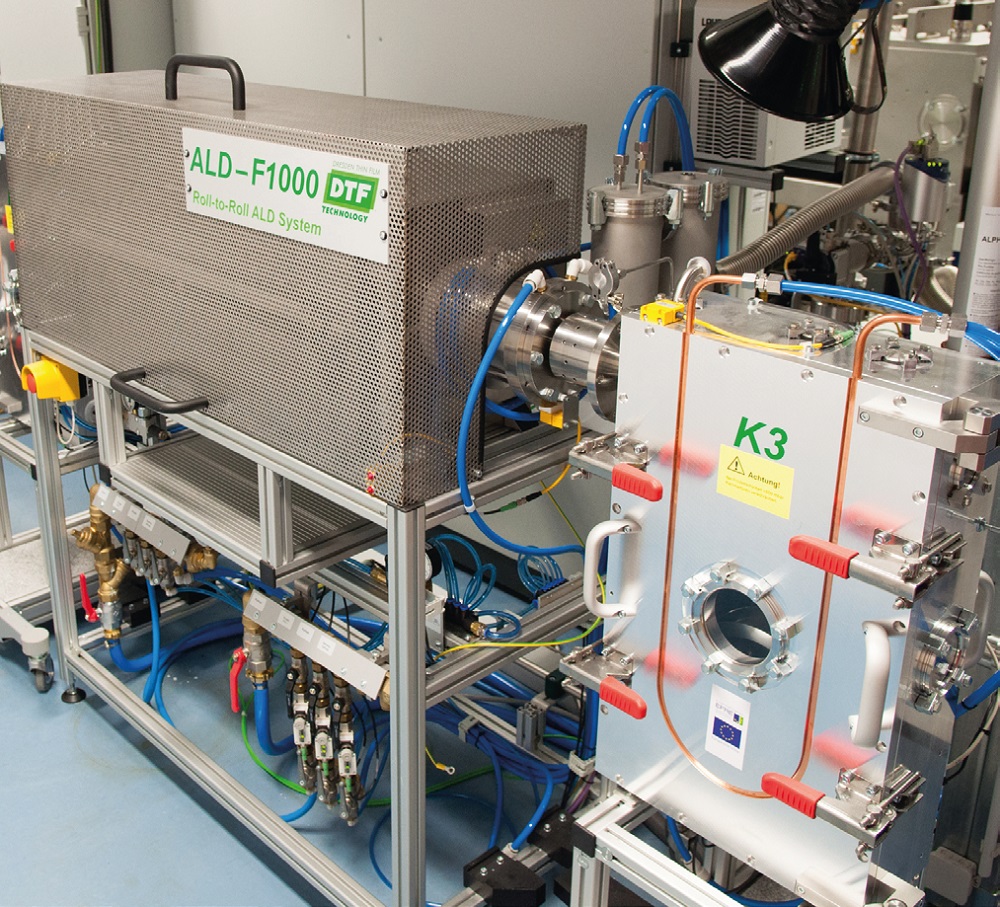
- Continuous roll-to-roll ALD of endless fibers and rovings
- Batch ALD for textile preforms
- ALD on particles and powders
- ALD barrier technology for displays, flexible electronics, and packaging
- Protective layers for tool applications
- Backside passivation for Si photovoltaics
