Superfast plasma-ald with 3D-printed ceramic rocket nozzles
Current research


Atomic Layer Deposition (ALD) for self-aligned multiple patterning has been the key process to the continued scaling of nanotechnology and microchips. The process requires plasma ALD at low temperatures and a conformal deposition of spacers on photoresist features for the subsequent pitch splitting processes. However, ALD is limited by low throughput, which can be improved by increasing the growth per cycle (GPC), using new precursor, spatial ALD, shrinking the ALD cycle length or omitting purge steps. Today’s highly productive platforms can realize very fast wafer transport in and out of the ALD chambers. Currently, 300 mm wafer ALD chambers for high volume manufacturing are used.
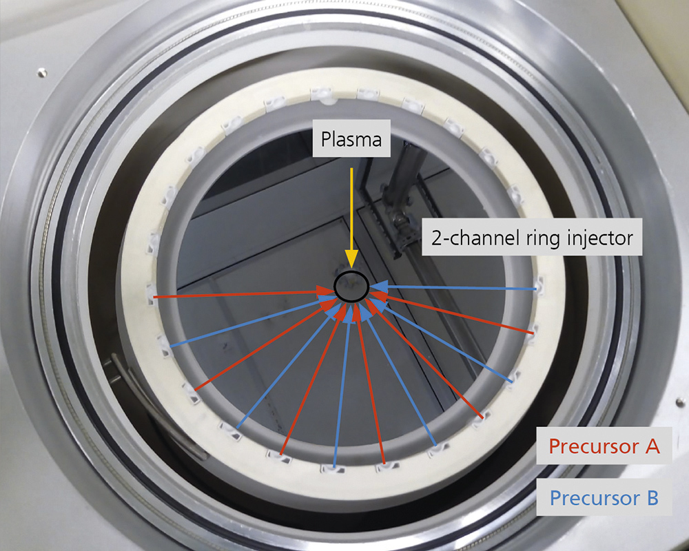
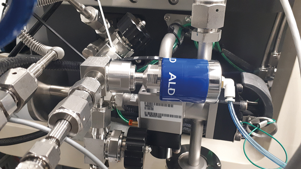
Fraunhofer IKTS, in collaboration with Plasway Technologies GmbH, has developed a new type of fast plasma ALD process. It uses a top-down showerhead gas flow to ignite a 60 MHz CCP plasma in a 300 mm chamber. The chamber gas system has been modified to realize precursor pulses of ≤ 10 ms with supersonic precursor gas injection. The supersonic gas speed is made possible by a 3D-printed ceramic rocket nozzle, named “Art de Laval”, manufactured and patented by Plasway Technologies, which enables high-speed (> 300 m/s), all-round precursor injection across the wafer. Initial process qualification was made with the well-understood aluminum oxide plasma ALD process using the trimethylaluminum precursor. With the de Laval ring injector, the saturation started at a TMA pulse length of 10 ms, which is the tested switching limit of the electropneumatic ALD valve. The process linearity and the saturation curve demonstrated the ALD nature of the process. For 50 ms of TMA pulse, a wide ALD temperature window (30–120 °C) with constant 1.3 Å GPC was extracted. Even with very short pulses, we achieved a very good uniformity of the applied layers – from wafer center to the edge.
Additional ALD processes, as well as atomic layer etching (ALE), will be the focus of future development efforts by Fraunhofer IKTS and Plasway Technologies GmbH.