
Scanning electron microscopy (SEM) often shows a very low material contrast when examining materials that differ only slightly in their composition. In addition, radiation-sensitive samples can be damaged during observation. In order to significantly reduce the volume of interaction in the electron microscope and to obtain essential information from the surface area of the sample, it is possible to use low primary beam energies (Ep). Through advances in field emission source design, aberration- corrected optics and improved detector sensitivity, modern low-voltage SEMs (LVSEMs) are now able to provide additional analytical information. The combination of the signal of the backscattered electrons with low primary beam energy opens up new imaging possibilities for the characterization of radiation- sensitive materials. This reduction of radiation damage is essential in particular for thin films, organic samples and some hybrid materials.
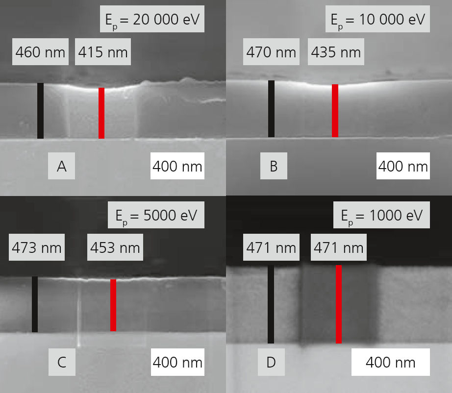
Thin films of organosilicate glass (OSG) are used in modern microelectronic products as low-k dielectric between the metallic conductors. If the glass network of the OSG interacts with the electrical beam, it can become denser, which leads to a significant shrinkage of the material. By combining low primary beam energy (Ep = 1000 eV) with the use of the energy-selective backscattered (EsB) detector, however, the compositional contrast between the OSG thin film and the Si substrate is increased and the shrinkage phenomenon is significantly mitigated (Figure 1).
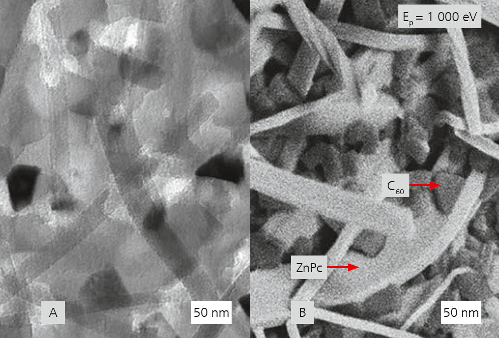
Characterizing the specimen morphology is a key step toward improving fundamental features of functional materials, such as the energy conversion efficiency of solar cells using organic photovoltaic thin films. With the EsB detector, only electrons with a certain energy (such as the backscattered electrons – BSE) can be used for SEM imaging. The low primary beam energy mitigates the charging effects for non-conducting specimens. Figure 2 shows an active zinc-phthalocyanine (ZNPC, donor) layer with embedded fullerene particles (C60, acceptor) used in bulk heterojunction for OPV cells. In Figure 2A, the transmission electron microscope (TEM) image of the ZnPc-C60 (fullerene, acceptor) does show a mix of long rods and smaller (brighter and darker) domains, but the two compounds cannot be identified. In contrast to this, the BSE image (Figure 2B) allows to differentiate between the ZnPc (bright long rods) and the C60 (dark nanoparticles), providing optimized SEM working conditions.
