TEM – A versatile technique for studying emerging materials
Current research


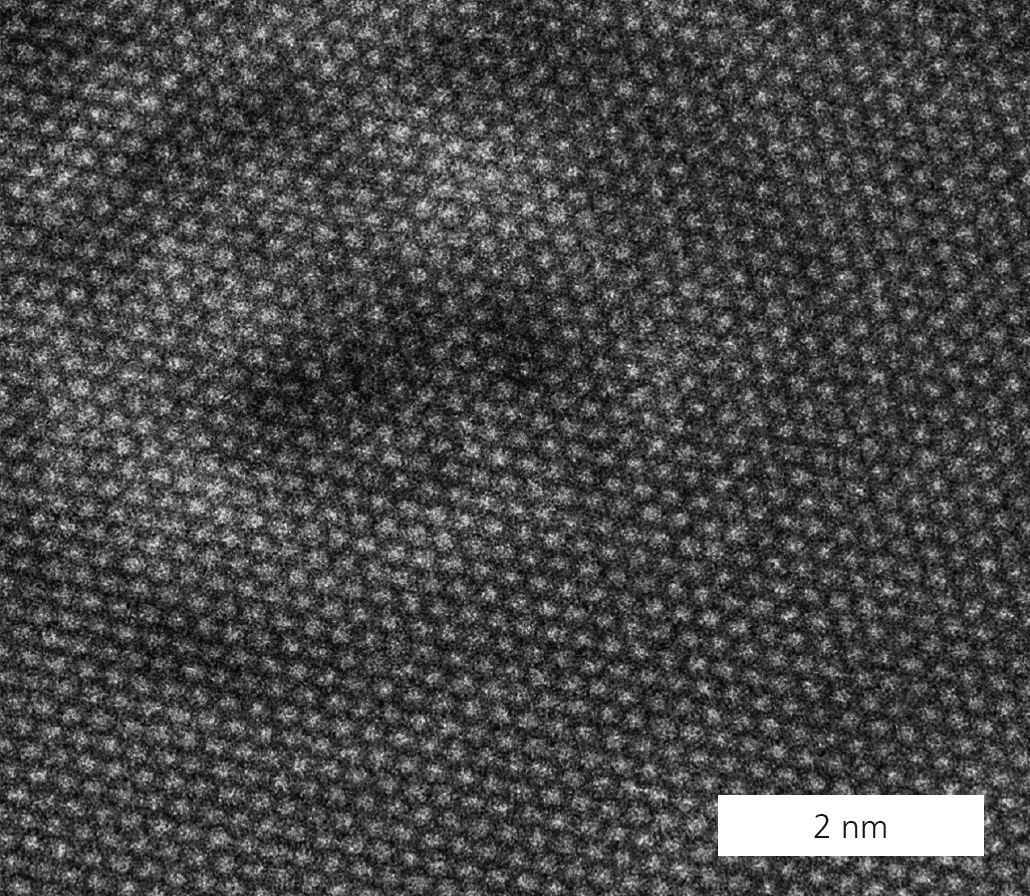
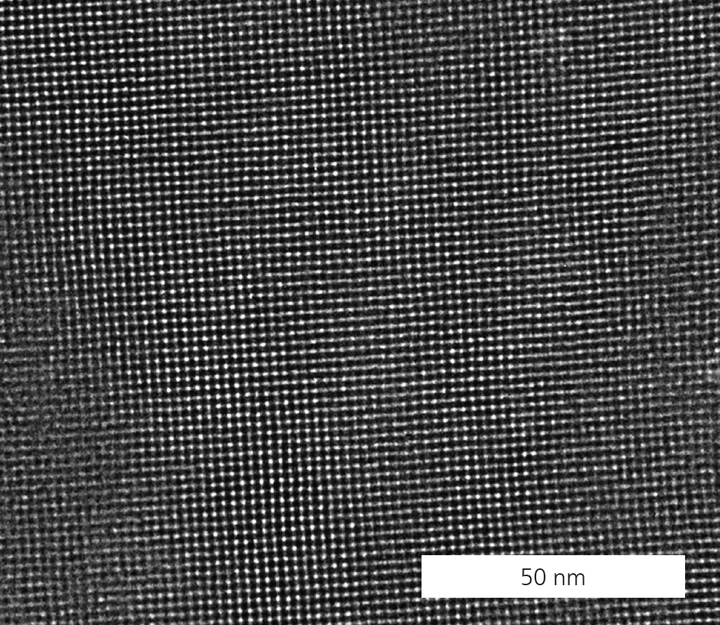
Transmission electron microscopy (TEM) uses the interaction between electrons and a material to characterize materials. The method provides insights into the microstructure, crystal structure, strain, defects, as well as composition (e.g. by energy-dispersive x-ray spectroscopy, EDS) and chemical bonding (electron energy loss spectroscopy, EELS) of the material. The resolution that can be attained by this method reaches down to the atomic level. TEM enables us to address many challenges in novel materials development, improving products properties and manufacturing processes, and supporting defect analysis and physical failure analysis.
High-resolution imaging and analysis of emerging 2D materials
Nanoelectronics, sensors and catalysts use beam-sensitive materials, e.g. graphene [1] and 2D polymers. Low-voltage TEM is used to characterize them. This means that the polymer molecules are not destroyed and can be measured directly in the high-resolution images. These images play a crucial role in guiding the synthesis process and understanding the electronic properties (e.g. electrical conductivity). TEM imaging combined with elemental analysis also provides structure information of electrocatalysts with fast water dissociation kinetics for energy storage [2]. The morphology and exact location of these nano-particles, which were determined in the study, explain the fast water-splitting performance, which is comparable to platinum.
Stress and in-situ studies to support reliability engineering in the semiconductor industry
Electron diffraction has been used to quantitatively determine the residual stress in the transistor channel caused by advanced packaging. In addition, in-situ capabilities have been successfully developed for reliability engineering in emerging products for microelectronics [3] and for band-gap engineering in graph-ene nanoribbons [1]. This enabled to observe the degradation process of dielectrics in the back-end-of-line (BEoL) structures in microchips, and to provide directions for strain engineered bandgap in 2D materials for sensor applications.
Analytical services offered
- High-resolution imaging (TEM and STEM), tomography
- Analysis in TEM (EDS, EELS, electron diffraction)
- In-situ TEM experiments (electrical, mechanical, heating up to 445 °C)
Literatur
[1] Z. Liao et al. Sci. Rep. 7, (2017), 211-1-7.
[2] J. Zhang et al. Nat. Commun. 8, (2017), 15437-1-8.
[3] Z. Liao et al. Microelectron. Eng. 137, (2015), 47-53.