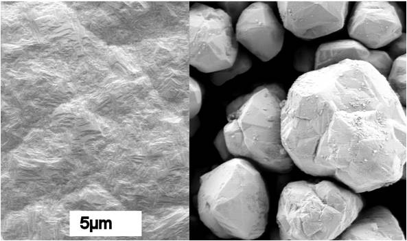


Microelectronics require highly conductive and stable circuit paths, often connected with additional constraints like high heat conduction of the substrate for a robust performance of the system. To avoid rising material costs (noble metals) in microelectronics different methods for metalization and their combinations are in development. Nevertheless, the combintaion of screen printing and electrolytic deposition gives rise to new demands on both techniques. In our group the influence of galvanic bath compositions on different thick films are investigated.
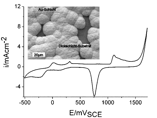
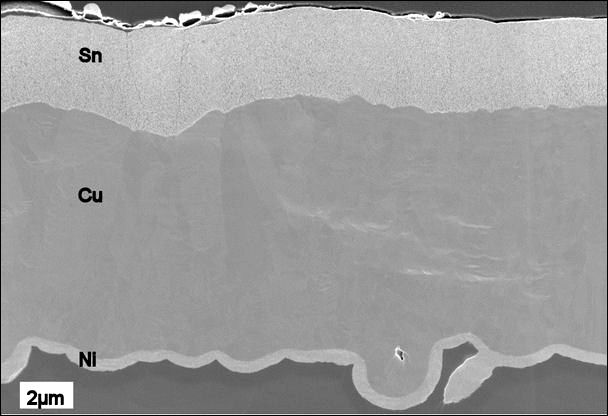
For power electronics electrolytic depositions with highly conductive copper circuit board tracks, allowing a good heat conduction, are in development. To save material costs for bonding gold layers electroless nickel and gold depositions are on duty. A complete covering of the thick film has to be achieved and tested to ensure good bonding performamce.
Dispersion layers of gold and ceramic nano particles are in development for wear protection and to increase the reliabilty of gold contacts.
Services offered
- Development of procedures for electrolytic and electroless depositions
- Electrochemical and microscopical characterization of electrolytic layers