
Electromagnetic test systems and test methods

Products and services
Leading-edge technology for carbon textile testing, 3D inspection of electronic components, for test systems for process control and of large-scale industrial plants
Fraunhofer IKTS delivers electromagnetic test systems, components and on-site test methods for non-destructive testing of single parts as well as of large numbers of pieces in automated processes. The application know-how corresponds to electronics, software, sensors and manipulation.
Along with its EddyCus® high-frequency eddy current technology for carbon textile testing, Fraunhofer IKTS offers attractive license-based business models. In-house developed x-ray measurement technologies are available for 3D object inspections with very high spatial resolution. Test systems for application in process control and a non-destructive, low-effort micromagnetic test method for the evaluation of residual lifetime of large-scale industrial plants and buildings complete the electromagnetic test systems and methods offered by Fraunhofer IKTS.
- Industrial sensor systems
• EddyCus® MPECS – imaging technology for the evaluation of carbon fiber layers
• Texture analysis of CFRP at arbitrarily formed structures
• EddyCus® Wetcoating – characterization of the drying behavior of conductive films
• X-ray line detector L100e® – directly converting, counting X-ray detector
- Sensor system components
• Eddy current and high-frequency eddy current detectors and arrays
• Customized electronics
• Customized software
- Measurement and testing services
• X-ray computed tomography and x-ray laminography
• X-ray microscopy and nano x-ray computed tomography
• Industrial microcomputed tomography
• X-ray diffraction
• Eddy current testing
• Micromagnetic testing
Industrial sensor systems
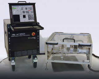
EddyCus® MPECS – imaging eddy current measurement for the evaluation of carbon fiber layers at 3D structures
EddyCus® MPECS is a universally configurable eddy current scanner for fast process-oriented random sampling of (3D) structures of carbon fiber composites. The eddy current-based test method uses the electrical properties of carbon fibers for quality evaluation and works couplant- and radiation-free.
Besides single components, Fraunhofer IKTS delivers complex sensor systems with its EddyCus® high-frequency eddy current technology for carbon textile testing. Thereby, various materials can be non-destructively tested and monitored via eddy current, high-frequency eddy current and imaging impedance spectroscopy in a frequency range from 100 kHz to 100 MHz. The in-house developed EddyCus® platform is applied for e.g. characterization of the hardening process of epoxy resins or the electrical evaluation of ceramics. Moreover, metallic materials, fiber composites (CFRP), ceramics (SiC), plastics and other, even weakly conductive materials can be tested.
For more information on the EddyCus® MPECS, please contact:
Prof. Dr.-Ing. Henning Heuer
Department: Systems for Testing and Analysis
Texture analysis of CFRP at arbitrarily formed structures
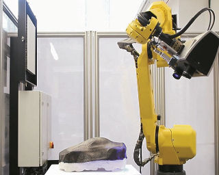
Industrial robots are the core of flexibly applicable test systems for complex 3D structures. Unknown objects are digitalized by stripe light projection. It includes scan path planning and programming. By scanning arbitrarily shaped surfaces, simulation results can be compared to measurements regarding real components. For example, the structure of carbon fiber layers becomes visible by using high-frequency eddy current. This structure can be quantified by texture analysis of curved surfaces, e.g. angles between layers, lane widths, distributions or anomalies.
For more information on texture analysis, please contact:
Prof. Dr.-Ing. Henning Heuer
Department: Systems for Testing and Analysis
EddyCus® Wetcoating –characterization of the drying behavior of conductive films
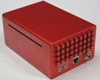
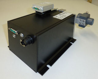
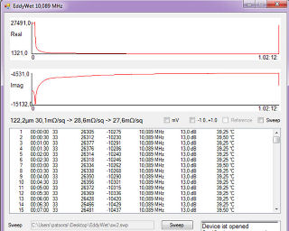
With EddyCus® Wetcoating, drying curves can be recorded and visualized for wet, thin and weak conductive layers at frequencies of up to 100 MHz. Thereby, the final properties of conductive layers can be predicted while still in the wet state. Drift influences of temperature, measurement setup or electronic components are permanently compensated. Fraunhofer IKTS delivers an easily transportable device, which includes an internal sensor for determining drying parameters as well as a manual sensor for surfaces at a measuring distance of up to 5 m from the device.
For more information on EddyCus® Wetcoating, please contact:
Prof. Dr.-Ing. Henning Heuer
Department: Systems for Testing and Analysis
X-ray line detector L100e® – directly converting, counting x-ray detector
The x-ray line detector L100e® solves complex tasks in the area of non-destructive testing with an unmatched quality. It comprises energy discrimination, single photon counting, high resolution as well as flexibility and speed. Besides its actual application – the detection of x-radiation – the line detector L100e® can also be adapted to optical test tasks (process control, sorting, tomography).
L100e® is just one of the possible configurations of the sensor system. Other applications include very long as well as curved detectors. Moreover, special configurations can be realized for proving high counting rates.
For more information on the x-ray line detector L100e®, please contact:
Dr. Peter Krüger
Department: Accredited Testing Laboratory
Sensor system components
Eddy current and high-frequency eddy current detectors and arrays
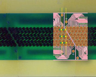
Based on parameter studies, e.g. regarding novel materials, Fraunhofer IKTS determines suitable parameters and delivers customized eddy current and high-frequency eddy current detectors. They can be applied for in-line testing, role-to-role methods, grid pattern generation, one-sided free-form scans of curved objects or used as load indicators. To achieve a high test throughput, the detector arrays are individually adapted to the geometries. Prior parameter studies can be accompanied and verified by other non-destructive test methods in the in-house accredited test lab on demand.
For more information on detectors and arrays, please contact:
Prof. Dr.-Ing. Henning Heuer
Department: Systems for Testing and Analysis
Customized electronics
Fraunhofer IKTS designs and builds all components required for automated measuring procedures. Among them are e.g. deposited preamplifiers, multiplexers and circuit boards of the detectors (arrays). For integration into production and test equipment, the periphery of wiring, computer technology and installation materials are individually compiled.
For more information on customized electronics, please contact:
Prof. Dr.-Ing. Henning Heuer
Department: Systems for Testing and Analysis
Customized software – EddyCus® MPECS and EddyCus® Integration Kit
EddyCus® MPECS (Multi Parameter Eddy Current Scanner), in connection with a Cartesian test system for planar samples, and the EddyCus® Integration Kit, e.g. for the adaption to a robot, include a software for controlling the measurement data acquisition as well as the evaluation and administration of the data. Nearly all established interface specifications can be integrated. On request, database interface, user administration und automated report creation can be added, too.
For more information on customized software, please contact:
Prof. Dr.-Ing. Henning Heuer
Department: Systems for Testing and Analysis


Measurement and testing services
Eddy current testing for defect analysis
The eddy current method is a fast and simple electromagnetic test method. A coil induces a small alternating field in the electrically conductive material. From the interaction in the material, surface defects, layer thicknesses and geometric properties can be derived. Resolutions differ considerably depending on task, geometry and material.
Fraunhofer IKTS offers eddy current testing with the following services:
- Development, optimization, test and validation of new test methods including simulation calculations
- Manual eddy current testing of components of various geometries
- Eddy current scans, also with high spatial resolution (approx. 200 µm), of flat components
- Testing for surface defects, determination of conductivity after calibration as well as layer and wall thickness measurements
- Examinations with different sensors (absolute, differential), measurement frequencies of up to 100 MHz
For more information on eddy current testing, please contact:
Christoph Prüfer
Group: NDT Test Lab
Micromagnetic testing – evaluation of the residual lifetime of large-scale industrial plants and buildings
Environmental influences cause materials fatigue in nearly all large-scale industrial plants over time. If exogenous overload is not perceived in time, the operators of ferromagnetic large-scale plants (power plants, public utilities, antenna and radio facilities or civil infrastructures) are threatened by failure of components or even the whole plant.
A permanent monitoring of large-scale plants has been time- and cost-intensive so far. This is changing due to the introduction of in-situ damage characterization for all ferromagnetic materials, which can be caused by cyclic or static deformation. Statements concerning materials fatigue, hardness, hardening depth as well as stresses contribute to a realistic estimation of the residual lifetime and enable in-time measures, like maintenance or replacement of the components concerned.
For more information on residual lifetime prognosis of ferromagnetic components, please contact:
Christoph Prüfer
Group: NDT Test Lab
X-ray microscopy and nano x-ray computed tomography
For the materials sciences, energy engineering, microelectronics and biomedicine, Fraunhofer IKTS offers x-ray microscopy for the non-destructive analysis of structures and defects in materials or biological objects.
The process enables the investigation of structural as well as functional materials, facilitates in-situ x-ray microscopy monitoring of chemical processes in miniaturized reaction chambers on a microscopic level, provides detailed images regarding analyses of microelectronic products, or used for the investigation of biological structures by allowing substructures of biological cells to be imaged.
For even more detailed images of specific structure parts, Fraunhofer IKTS uses nano x-ray CT (Nano-XCT). With this method, the morphology and topology of the regions of interest can be imaged three-dimensional. Thus, nano x-ray CT supports e.g. the localization of delaminations and cracks after loads on composite materials, in the field of materials science, or the detection of pores below 100 nm in diameter in copper TSV structures of high-performance chips of the microelectronics industry.
X-ray optics are continuously enhanced by Fraunhofer IKTS. With the manufacturing of multilayer Laue lenses, which have already been successfully integrated into laboratory x-ray microscopes for full-field images, resolutions of 10 nm shall be achieved. Thereby, even smaller structures can be analyzed in the future, e.g. regarding ultra-modern chips whose wiring structures on chip level have arrived at dimensions of 100 nm and below.
Fraunhofer IKTS offers the following services:
- High-resolution 2D und 3D x-ray microscopy
- Investigation of kinetic processes, in-situ experiments: temperature chamber, chemical reaction chamber, mechanical micro DCB test
- Imaging with absorption and Zernike phase contrast
- Highest resolution up to a minimum pixel width of 32 nm
- Acquisition and reconstruction of 3D and 4D data sets: tomography, laminography, image series and time-resolved tomography
- Data evaluation, segmentation
For more information on x-ray microscopy and nano XCT, please contact:
Dr. Jürgen Gluch
Department: Microelectronic Materials and Nanoanalysis, Group: Micro- and Nanoanalysis