 Fraunhofer Institute for Ceramic Technologies and Systems IKTS
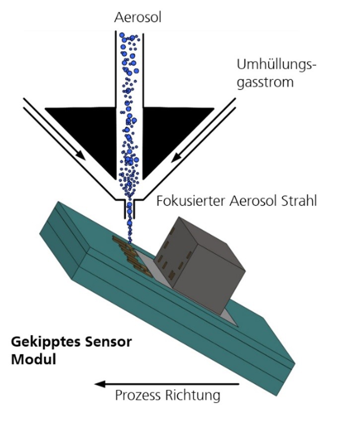
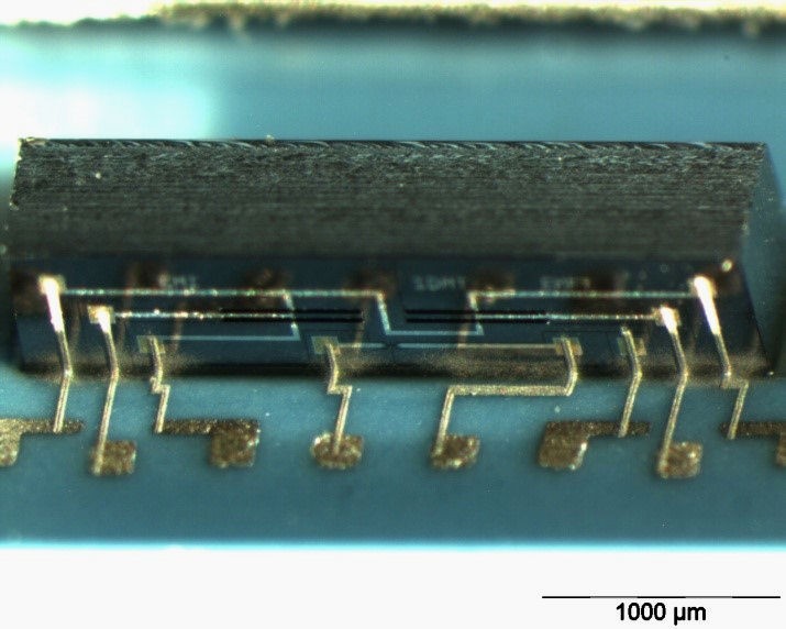
Chip contacting above an adhesive ramp
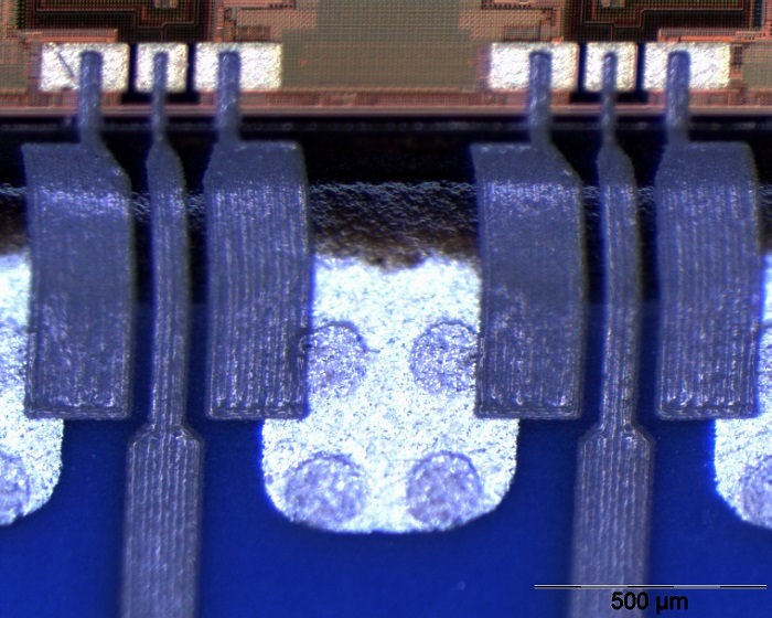
90 ° 3D-contacted g-accelerometer MEMS
Printed coplanar line for MMIC
Si-Microchips and MEMS are typically contacted by wire bonding, flip chip bonding or by a TAB process. Applications which are not wire or flip chip bondable (e.g. on flexible substrates, complex MEMS geometries, MMICs, HF applications) require an alternative solution: Direct writing solutions. Therefore a low temperature sintering ink will be printed from the top side chip pads above an adhesive ramp to the substrate carrier (PCB, ceramic substrate, flex circuits). The printing technology provides benefits in comparison to the traditional methods:
- Reduction of space consumption,
- Wire bonds – prevention of parasitic inductance (loops),
- Optimal RF modulation (printed coplanar conductors),
- Minimal chip pad dimension –> enhanced chip contacts possible,
- Contacting of mechanical and thermal sensitive chips (ultra-thin chips) and
- contacting over edge till 90° possible.
Technical characteristics:
- Printed Interconnects down to Line/Space 10 µm,
- Substrates: PCB, Ceramic, Flex (Polyimid, Teflon, PET) and
- Ag- and Au-Inks as well as thermomechanically adapted adhesive.
Services offered:
- Development of chip contacting solutions for different substrate types,
- Consulting in material selection for direct written interconnects.