Fraunhofer Institute for Ceramic Technologies and Systems IKTS
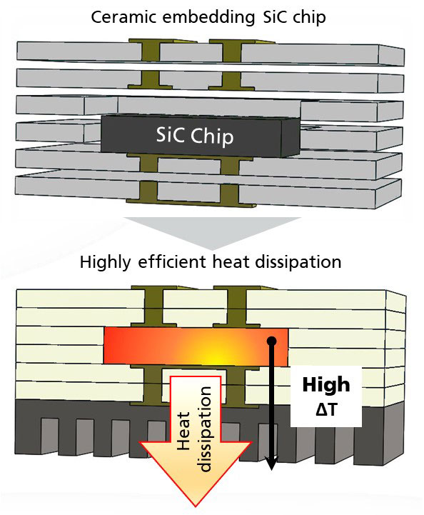
SiC-based semiconductors are currently used in the form of diodes and transistors. In conventional assembly and connection technology, the semiconductor is soldered or sintered onto a metallized ceramic substrate, with electrical contacting on the top using wire bonding technology. For encapsulation, the semiconductor can be encapsulated with a plastic. Regardless of the type of semiconductor, the current packaging and connection technology (housing, potting compound and terminal contacts) can only be operated at temperatures of up to 200 °C for a short time and up to 150 °C for a long time. In addition, the currently used housing materials have poor corrosion resistance and inappropriate thermal linear expansion.
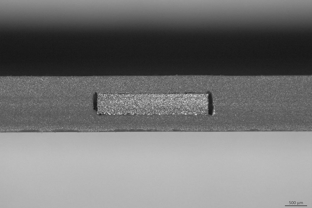
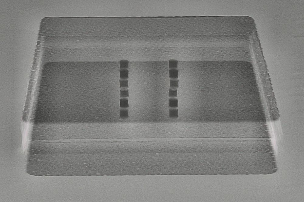
To solve these problems, Fraunhofer IKTS is working on high temperature stable assemblies. For this purpose, the semiconductor components are embedded in a multilayer ceramic package under ceramic-specific firing temperatures, sintered and simultaneously electrically and thermally contacted. Integration in ceramic or ceramic-compatible materials represents a high-temperature-stable packaging technology that allows the potential of the wide bandgap semiconductor materials used (switchable currents/current densities, maximum operating temperatures, device miniaturization) to be exploited to the full.
The SiC semiconductor device is integrated into a pre-metallized and pre-structured green film stack using ceramic green films. A monolithic ceramic pre-package with embedded SiC device and ceramic-integrated electrical rewiring is produced by pressure-assisted sintering of the ceramic.
Depending on the temperature stability of the semiconductors, various ceramic materials are available for embedding the semiconductor devices. Embedding in an LTCC-based dielectric base ceramic (Low Temperature Cofired Ceramics) is currently performed at minimum sintering temperatures of 750 °C with a holding time of 2 h. However, the high temperature load on the contact metallization of the semiconductor devices during the sintering process can lead to degradation or limitation of the electrical performance of the semiconductor devices. Further development of the manufacturing process using the dielectric ULTCC (Ultra Low Temperature Cofired Ceramics) base materials developed at Fraunhofer IKTS allow a further reduction of the sintering temperature to 480 °C with a holding time of 30 min.