 Fraunhofer Institute for Ceramic Technologies and Systems IKTS
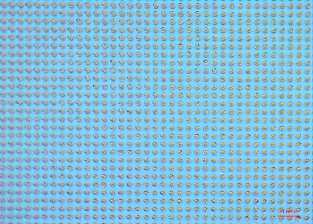
High wiring density multilayer ceramic circuit board manufactured in LTCC
Ceramic circuit boards are mechanical carriers, upon which conducting structures for the wiring of electronic components are deposited. Besides providing electrical connections for microelectronic components they have a supporting function, a thermal function (heat removal) and a protecting function (atmosphere, particles, electromagnetic radiation). A fundamental differentiation into single layer carriers, double layer carriers, multilayer carriers and carriers manufactured by multiple deposition processes is possible. As manufacturing technologies Printed Circuit Board Technology (rigid/flexible), Thick Film Technology und Multilayer Ceramic Technology is in use.
Multilayer ceramic circuit boards have following advantages compared to alternative solutions:
- High wiring densities (Number of wires per area of substrate) due to high resolution thick film based printing processes, due to highly miniaturized electrical through contacts and due to wiring on different layers of the multilayer (R & D > 40 Layer),,
- High packaging density (area of assembled electrical components per substrate surface) by integration of passive components (R, L, C) on the inner layers of the multilayer substrate,
- Stability under high mechanical load like vibration and shock,
- Thermomechanical adaption of the ceramic substrate to the silicon based components (high reliability during thermal cycling),
- Optimal heat removal for power electronic components due to good heat conductivity of the ceramic in combination with excellent stability under increased temperatures and
- True hermetic sealing of sensible electronics by covering/capping in combination with inorganic joining technologies.
Current developments of Fraunhofer IKTS are aiming to increase the state of the art wiring densities of the LTCC-Technology by the usage of new structuring and deposition technologies. Exemplary are the design rules of commercial multilayer ceramic manufacturers with line width/space (Line/Space) of 0.1/0.1 mm and minimal via diameters of 0.15 mm, which have to be reduced.
By using advanced punching technology for the structuring of via holes smallest via diameters of 0.1 mm are technically feasible. The usage of laser technology allows for a further miniaturization of via diameters down to 0.06 mm. By adapting the rheology of the via-fill pastes and by improving the printing technology the vias can be filled successfully.
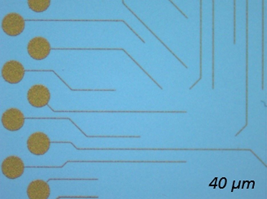
By modification of the screen printing pastes and by using fine-line screen-printing technologies high resolution conductors were deposited on green ceramic tapes. Minimum line width of 0.04 mm (fired, substrate size 4”x4”) can be manufactured.
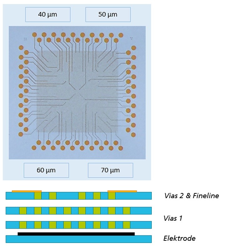
To illustrate the technological possibilities both technologies were combined within one demonstrator.
Technical data:
- Multilayer ceramic circuit board
- Substrate thickness 0.4 mm (sintered)
- Via diameters > 0.06 mm
- Via distance (edge to edge) 0,09 mm
- Conductor width > 0.04 mm
Services offered:
- Customer service concerning manufacturing options in LTCC
- Custom-built design
- Elaboration and qualification of manufacturing processes
- Manufacturing of samples
- Technology transfer