 Fraunhofer Institute for Ceramic Technologies and Systems IKTS
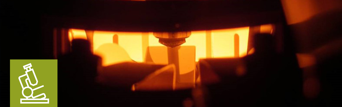
Materials and Process Analysis
Areas of application
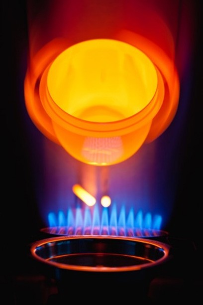
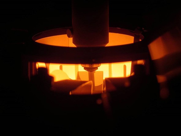
Sample fusion apparatus for raw material analysis.
Raw materials analysis and evaluation
Detailed knowledge of the materials used and their processing characteristics is paramount to the development and optimization of stable, economical and sustainable production processes, thus resulting in products of superior quality. Fraunhofer IKTS assists clients and project partners with analysis and evaluation of materials on a scale spanning the nm to mm range, conducted at the institute or at client/partner premises. Researchers study materials that run the gamut from oxide ceramics, non-oxide ceramics and hardmetals to carbon-based materials and glass or organic raw materials (certified according to DIN EN ISO/EC 17025).
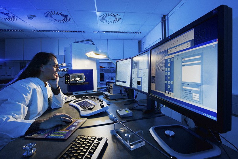
Scanning electron microscopy with dual-beam device (Zeiss NVision 40 with EDX and EBSD system).
Characterization along the entire process chain
Fraunhofer IKTS has the expertise and the tools to provide characterization at every step of processes involving ceramic, powder metallurgical, and associated technologies – from preparation and conditioning of raw materials, suspensions, and pastes to drying and granulation, shaping and thermal treatment to finishing. The data collected from such characterization can be directly applied to the analysis of individual process steps or to the properties of semi-finished products. These data are also useful in establishing methods for process and product monitoring, and as a basis for process modeling.
Heat durability testing (recipient of test stand at 1000 °C).
Materials and component characterization
Knowledge of the micro-scale and nano-scale structure of the material and its changes during application are essential to predict and ensure product quality and lifetime, even under extreme loads. In this regard, Fraunhofer IKTS has the capability to analyze the microstructures and properties of materials and components subjected to a broad range of temperatures. Fraunhofer IKTS supports its clients from the preparation of test samples through to interpretation of the determined properties. In addition, it has comprehensive experiences that ranges from analysis and evaluation of aging processes to evaluation of failure of ceramic components. This makes it possible to optimize high-performance ceramics, hardmetals and cermets, super hard materials, graded materials, metal-ceramic composites, and materials for microelectronics and nanoelectronics. The institute uses its vast expertise to study the corrosion phenomena that influence ceramic materials and to model, simulate and optimize materials and components exposed to high temperatures of up to 2400 °C.
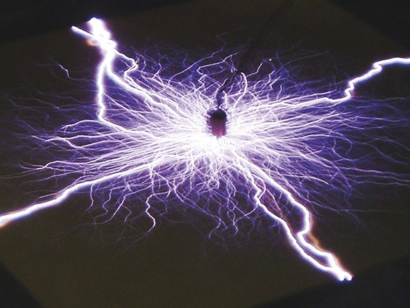
High-voltage testing.
Component and systems performance
Component lifespan and reliability must be studied in light of the conditions of their future use within the system. Fraunhofer IKTS offers a comprehensive selection of thermo-mechanical, chemical, electrical, physical, and climatic test processes to elucidate failure mechanisms, optimize products and achieve certifications more swiftly. Its primary focus is on structural and functional ceramic components, hardmetals, cermets, components of high-performance electronics and sensor systems, components based on composite materials, and components used in filtration and catalysis. The comprehensive expertise on materials and technology forms the basis for substantial analysis of defects and permits lifetime predictions of components under the conditions to which ceramics are exposed. In addition to test planning, testing, and evaluation, Fraunhofer IKTS offers its clients specific in-line and off-line test stands and highly specialized, application-specific testing.
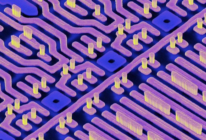
Microelectronic circuitry.
Analytics for micro- and nanoelectronics
Fraunhofer IKTS specializes in application-based physical microanalysis and nanoanalysis with the aid of which technical and design solutions are developed for microelectronics, nanoelectronics, and optical electronics. New materials and production technologies demand innovative concepts in order to ensure performance and reliability as electronic applications become increasingly sophisticated. Thanks to many years of experience and its vast array of technical equipment and facilities, Fraunhofer IKTS is uniquely capable of qualifying known analytical methods, and its in-house developed methods, for use in services and equipment developments. In addition to high-resolution processes of ion and electron microscopy, and X-ray technologies, Fraunhofer IKTS also investigates new approaches to the analysis of mechanical properties on the micro and nano levels. It applies and advances new methods to characterize electrical and mechanical mechanisms of degradation in situ.
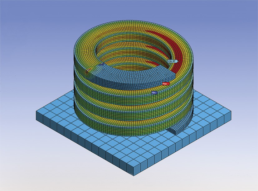
Stress distribution inside a ceramic spring.
Modeling and simulation
It is possible to curtail product cycles dramatically, and to minimize development risks, by simulating material properties, components, production technologies and systems environments. Even in the early development phases, the Fraunhofer IKTS team has access to software resources (FEM, CFD, systems simulation) for the simulation of thermal, mechanical and electrical processes, along with fluid-mechanical and reaction-technological processes in components and systems. With many years of experience in the use of flexible programming tools, the institute can also prepare and analyze user-specific model descriptions for new kinds of applications, particularly using coupled mechanisms (coupling matrix analyses, multiphysics).