Authors: Kathrin Reinhardt, Martin Ihle, Paul Gierth | Translation: Stephanie Anderseck
Printed electronics for highest frequencies: 6G wireless communication technology and millimeter wave radar
Mobile communication technology is less than 25 years old and has already taken several decisive steps in its development. New wireless communication standards are released on a regular basis and achieve ever higher transmission rates. UMTS is gradually being replaced first by 4G and finally, at present, by 5G. Due to the wide frequency spectrum of the 5G standard, in particular machine networking and digital images of reality can be generated, in addition to mobile radio applications. The computing power and storage capacity required for this are available in high market readiness. But for applications such as autonomous driving, much higher data rates are needed. The global goal is to increase the data rate from 20 gigabits per second at a latency of 1 millisecond (5G) to a full 1 terabit per second at a latency of just 0.1 millisecond (6G) by 2030. Ceramic substrate materials and adapted thick-film pastes and inks can make a significant contribution here.
Influence of substrate and conductor materials on high-frequency properties
An interconnect device must transport the electrical signal between functional semiconductor materials and antenna structures. The decisive factor here is the way in which the nature of the electrically conductive structures influences the electrical signal. In conventional applications without high frequencies such as LEDs, only the electrical resistance of the current-carrying structures is decisive. However, if the signal frequency is now increased, the electric current flow is increasingly accompanied by an electric or magnetic field. These fields surround the conductor and, like the electric current, must be guided in a defined manner. Thus, the material properties and the structure of the environment around a high-frequency conductor play a decisive role for the signal quality. If these parameters are inadequately designed, the high-frequency signal will be attenuated, resulting in a reduced data transmission rate for the end user.
The attenuation or high-frequency transmission losses of lines are composed of conduction losses of the conductor materials and dielectric losses of the substrate materials. Dielectric loss is the amount of electrical energy that results from conversion to heat in the dielectric when an electric field is applied. For microstrip lines, for example, from a frequency of about 1 GHz, the influence of the dielectric loss on the total loss increases significantly with increasing frequency compared to the conduction loss. In addition to a low permittivity, it therefore makes sense to use dielectric materials with a low loss angle (tan delta), which is incorporated proportionally into the dielectric loss.
Since the accompanying electric fields increasingly penetrate the substrate material as well, its properties are crucial. This is where the substance-dependent permittivity in particular comes into the play. It describes polarization effects in the dielectric substrate material, which counteract the electric field. Thus, a high permittivity value means increased signal attenuation. Like most material parameters, the value is not constant, but can change depending on the ambient temperature and also the frequency of the applied electric field.
Conventional dielectric PCB materials such as FR4 perform well in the lower frequency range. However, if the operating frequency increases, additional dielectric materials such as Rogers RT/duroid® laminates must increasingly be integrated into the substrate carrier. Such laminates cover a large part of all substrate materials for high-frequency applications so far. However, the material properties in the (sub-)terahertz range are not yet sufficient for 6G applications.
Ceramic LTCC substrate materials for low loss high frequency circuit carriers.
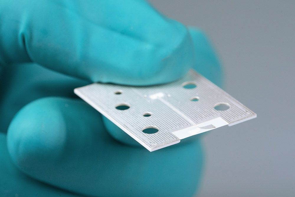
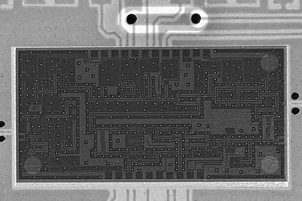
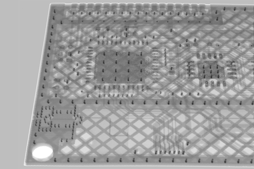
With their outstanding high-frequency characteristics such as a very low loss angle and a low permittivity number, all-ceramic or glass-ceramic LTCC materials offer the springboard to the next generation of circuit carriers. LTCC ceramics (low-temperature co-fired ceramics) can be functionalized in a manner comparable to printed circuit boards with electrical conductors and have internal functional layers or buried structures in multilayer technology. This results in several advantages. Both passive and active components can be fully embedded in ceramic cavities. In addition, self-supporting structures can be manufactured cost-efficiently and thus, for example, highly efficient antennas can be implemented directly on the circuit carrier or in the component housing.
One main difference between printed circuit board and ceramic substrate materials is the thermal behavior. LTCC ceramics have significantly lower thermal expansion behavior compared to classic printed circuit board materials. This means that they are much closer to the mostly directly attached circuits. Since the thermal expansion differs only slightly even in the case of heating, the mechanical stresses between the components are also lower. This has a positive effect on the reliability of the product. In addition, LTCC ceramics can also conduct heat much better than printed circuit boards. This allows highly stressed circuits to be deheated more efficiently and the entire assembly to be miniaturized.
Ceramic solutions have been investigated for the manufacture of high-frequency assemblies for several years now. In the meantime, it has been possible to demonstrate ceramic circuit carriers with consistently low dielectric losses in the D and H frequency bands (100 - 300 GHz), which are urgently needed for 6G applications. For this purpose, cost-effective, mass-market and reliable technologies based on LTCC multilayer technology were developed and characterized. The decisive factors here were the miniaturizability and structural stability of the electrical conducting tracks.
Deposition of miniaturized conducting tracks and antennas on a micrometer scale
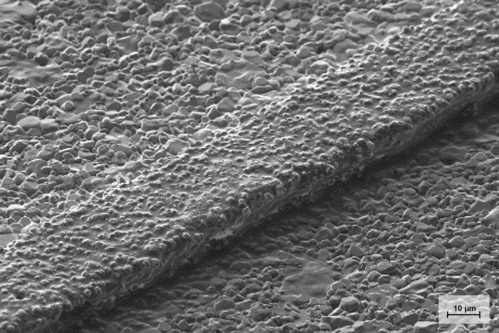
At high signal frequencies, the electric current no longer flows in the entire available conductor, but increasingly shifts to the outer conductor wall. This effect is called skin effect. For substrate-based microstrip conductors, it is crucial to realize a low edge roughness, even for structure widths smaller than 50 µm. Different processes are available for the production of such conducting tracks.
Laser structuring
For coplanar conductors, i.e. conducting tracks that are shielded by surrounding conductive structures, laser structuring can be used, among other things. In this process, a laser beam is used to remove material from a previously applied metallization layer. With the help of this multi-stage process, electrical structures with the highest edge resolutions and a gap distance of 20 µm can be realized, which has a positive effect on the signal quality. However, the process has only moderate mass production characteristics.
Aerosol jet printing
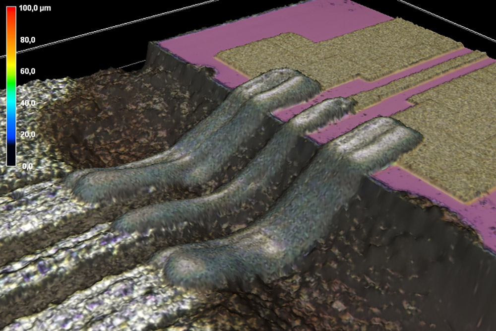
Gap widths of only 20 µm can also be achieved by means of aerosol jet pressure. In these processes, a solution of metallic particles and polymers is sprayed onto the substrate surface via ultra-fine nozzles. Since the material flow is so fine that one can no longer speak of a liquid jet, but rather of a material nebulization, the process is referred to as aerosol printing. This process also offers the possibility of printing three-dimensional surfaces. It is also being evaluated as a low-loss contacting technology between substrate carriers and mounted high-frequency microcircuits. As a result, connection methods that are not sufficiently reliable, such as flip-chip bonding or highly lossy wire bonding, can be substituted.
Screen printing
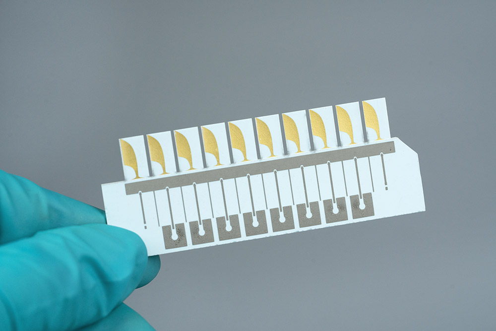
Since there is a high demand for assemblies to be served for the worldwide implementation of the 6G standard, high-throughput metallization processes such as thick-film technology must be applied. Ceramic circuit carriers are functionalized by screen printing as standard for the production of cost-efficient assemblies. For this purpose, so-called thick-film pastes are deposited on the surface by means of a structured pressure mask, the pressure screen, and sintered at temperatures of about 850 °C. The function of the thick film paste depends on its components and can be electrically insulating, chemically sensitive and/or electrically conductive. For electrically conductive pastes, ultra-fine metal particles are added as the main ingredient and homogenized with customized polymers and solvents.
The line width of a paste depends on a variety of factors. These include the material properties of the paste, but also the technological framework of the printing screen. A very low viscosity (colloquially thin) paste would bleed after screen printing and thus spread much wider than required. A very high viscosity paste would maintain its line width but would hardly relax after screen printing, resulting in a strong surface texture. The screen printing process itself is limited in terms of minimum screen openings. The screen fabric consists of a network of single threads at a defined distance. Technically, neither the threads nor the distance between two threads can be reduced endlessly, resulting in a natural limitation.
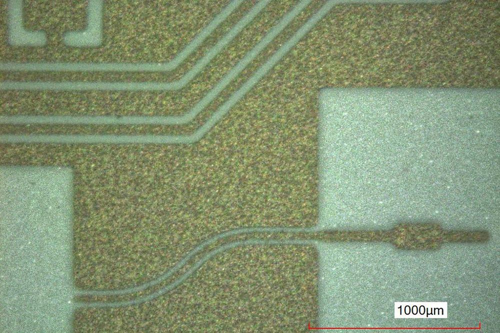
The current resolution limit of screen printing differs depending on the function. Technically simple and widely used are line structures between 150 and 200 µm for low-cost applications. Applications in the range < 100 µm become more demanding. For high-frequency applications, a line width of 30 µm can be achieved with standard equipment under laboratory conditions. This, however, exhausts the limits of the process. It is therefore suitable for comprehensive qualification of pilot applications, but a transfer to series production is associated with high requirements and is cost-intensive.
Structuring by means of photostructurable pastes
One way to overcome this technology hurdle is to adapt photostructuring for printed circuit board materials. For the metallization of printed circuit boards, a selective material removal from a full-surface coating is carried out instead of the additive process of screen printing, i.e., the selective material coating. In this subtractive process, the target layout is created on the PCB by selective etching of the copper. To allow etching to take place only at desired positions, the copper is coated with a photosensitive etch resist. This suspension, which is applied over the entire surface, hardens when exposed to light of a specific wavelength. If the light beam is only selectively applied through a shadow mask, the photoresist can be very finely structured. The material on non-illuminated areas can then be removed in a second process step. The structure resolution of this photomasking can be much finer than would be possible via direct screen printing.
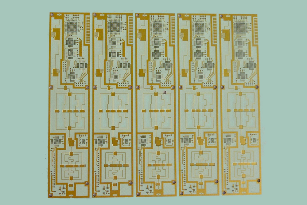
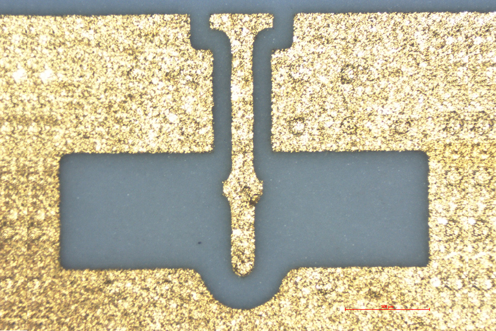
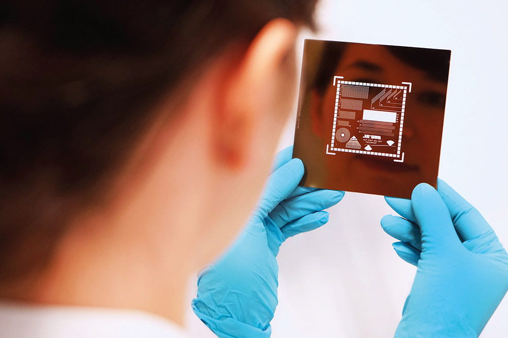
This technology can also be transferred to ceramic thick-film technology by means of photostructurable pastes (PI pastes). Here, the two sub-process steps of photostructuring - exposure and development - are implemented between layer deposition and thermal processing of the thick film. After full-surface or partially structured screen printing of the photosensitive thick-film pastes, they are selectively exposed after drying. Exposure can be achieved using either photomasks or maskless laser direct writing (LDI) techniques. This contributes to the digitalization of the process technology and to a further improvement in structural accuracy. The UV light used causes the polymer components to crosslink in a manner comparable to etching resist. This is followed by the wet chemical development process on an aqueous basis. This removes the areas of the layer whose polymers are not crosslinked - that is, which were covered by the mask. The assembly can then be fed into the conventional thermal sintering process. Although the actual metallization process for the entire assembly is extended by two steps, both steps can be easily integrated into an existing production line and require only about 15 to 30 seconds of additional process time.

The PI pastes are formulated to harden reliably under UV illumination but remain unaffected by daylight. A costly yellow room is therefore not necessary. The technology has already been successfully realized for silver and gold pastes. In addition, work is currently underway on copper, platinum, resistive and dielectric pastes.
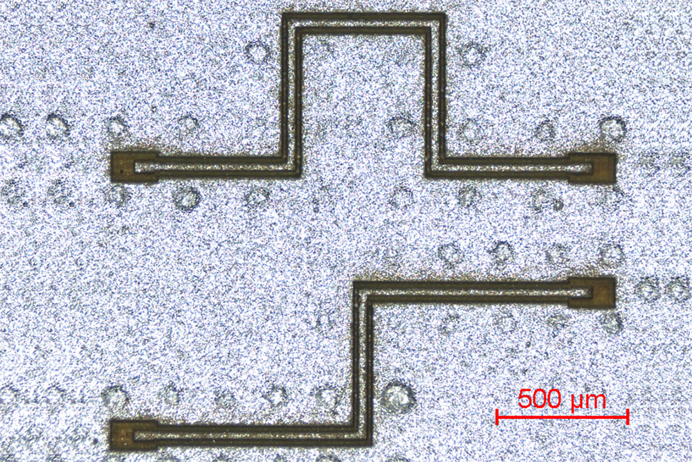
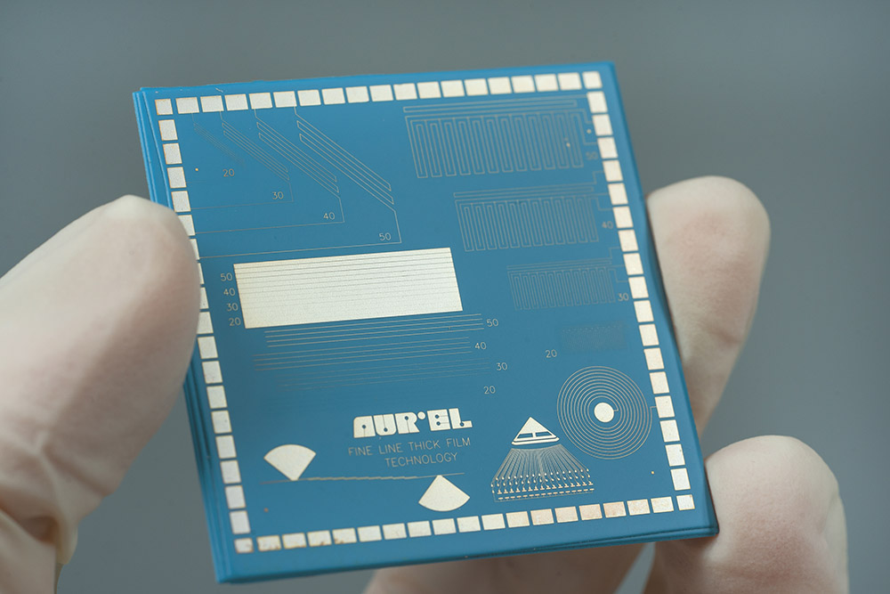
Using PI pastes, structural resolutions of 20 µm line width and line spacing can currently be achieved. Thus, the major technological requirements of the high-frequency application can be fully served. It should be emphasized that, in addition to ultra-fine conductors, full-surface metallizations can also be deposited in the same process step. In the conventional screen printing process, this is usually only possible by means of double printing and thus represents a cost advantage.
Modular product solutions
A variety of technologies are available to the end user for the development of customized assembly solutions. In addition to the already widely known manufacturing processes, an application and even a cost advantage can be achieved in particular by modifying the materials, i.e. the ceramics or the thick-film pastes. Fraunhofer IKTS cordially invites interested companies to characterize the technologies with regard to their suitability for defined products and to jointly develop them further.
Download
Further information
- Radio frequency circuits
- Fraunhofer IKTS department "Microsystems, LTCC and HTCC"
- FraunhoferIKTS department "Thick film technology and functional printing"
Stay informed: You are welcome to subscribe to our newsletter, read our other blog articles and follow us on LinkedIn, Instagram and YouTube.
