Translation: Stephanie Anderseck
Additive glass shaping improves selectivity of photomultipliers
Photomultipliers are, for example, used in food production or medical laboratories to detect the tiniest impurities in brewer's yeast or tiny genetic fragments in blood samples. These are ultra-precise detectors that can capture and reliably measure light effects of very low intensity. In order for these optoelectronic sensors to be used much more widely in the future, the measurement technology company ProxiVision and engineers from the Fraunhofer Institute for Ceramic Technologies and Systems IKTS have jointly developed additively manufactured photomultipliers. This will allow the sensors to be adapted quickly and flexibly to ever new application scenarios.
In the interview, Prof. Dr. Rolf-Jürgen Ahlers (CEO ProxiVision GmbH), Dr. Tassilo Moritz (Head of department “Processes and Components”, Fraunhofer IKTS) and Dr. Jochen Schilm (Group manager “Join-ing technology”, Fraunhofer IKTS), give an insight how the research project began, which technological paths they took and what prospects they see for new applications.
How did the cooperation between ProxiVision and Fraunhofer IKTS come about?
Tassilo Moritz: Employees of ProxiVision had visited our booth at a powder metallurgy trade show. There, we had shown which new powder-technological shaping processes are now available for the material glass – and this aroused ProxiVision’s interest.
Rolf-Jürgen Ahlers: For this, it is necessary to know how we have shaped our photomultipliers until now: We heat glass tubes, bend them to shape and expand them at the back to form funnels. This does also imply that we are limited here in the geometric variety and fineness of the structures. This is how the idea was born to become more flexible through new manufacturing methods. The glass injection molding that IKTS had shown at the trade fair appeared promising at a first glance.
But this one has proven to be a dead end?
Tassilo Moritz: I would not say it like that. But in fact, we realized quite quickly that we can create such complex structures much better using additive manufacturing. The only remaining question was, which of the processes available to us, that we use for ceramics, would be the best for ProxiVision's glass component. That is why we jointly applied for project funds from the “Central Innovation Program for SMEs (ZIM)” and tested three different additive processes in the course of this ZIM project.
What processes were these specifically?
Tassilo Moritz: Among other things, we tried ”CerAM FFF”. The abbreviation ”Cer” already reveals that this technology was originally developed for ceramic components. AM stands for “Additive Manufacturing” and FFF for “Fused Filament Fabrication”. In this process, the 3D printer gradually lays glass filaments on top of each other to form the desired geometry, much like strands of toothpaste. This creates a so-called green body, which then shrinks to the required component size during sintering. The result here, however, was that FFF simply cannot produce the structural detail needed for a photomultiplier. In other experiments, we used ”CerAM MMJ”, also called ”Multi Material Jetting”. In this process, the component is built up from tiny droplets in which glass powder and thermoplastic binders are mixed. However, the surface of the components produced with this method was too rough for the intended use.
And the third AM method finally won the race? What were the advantages?
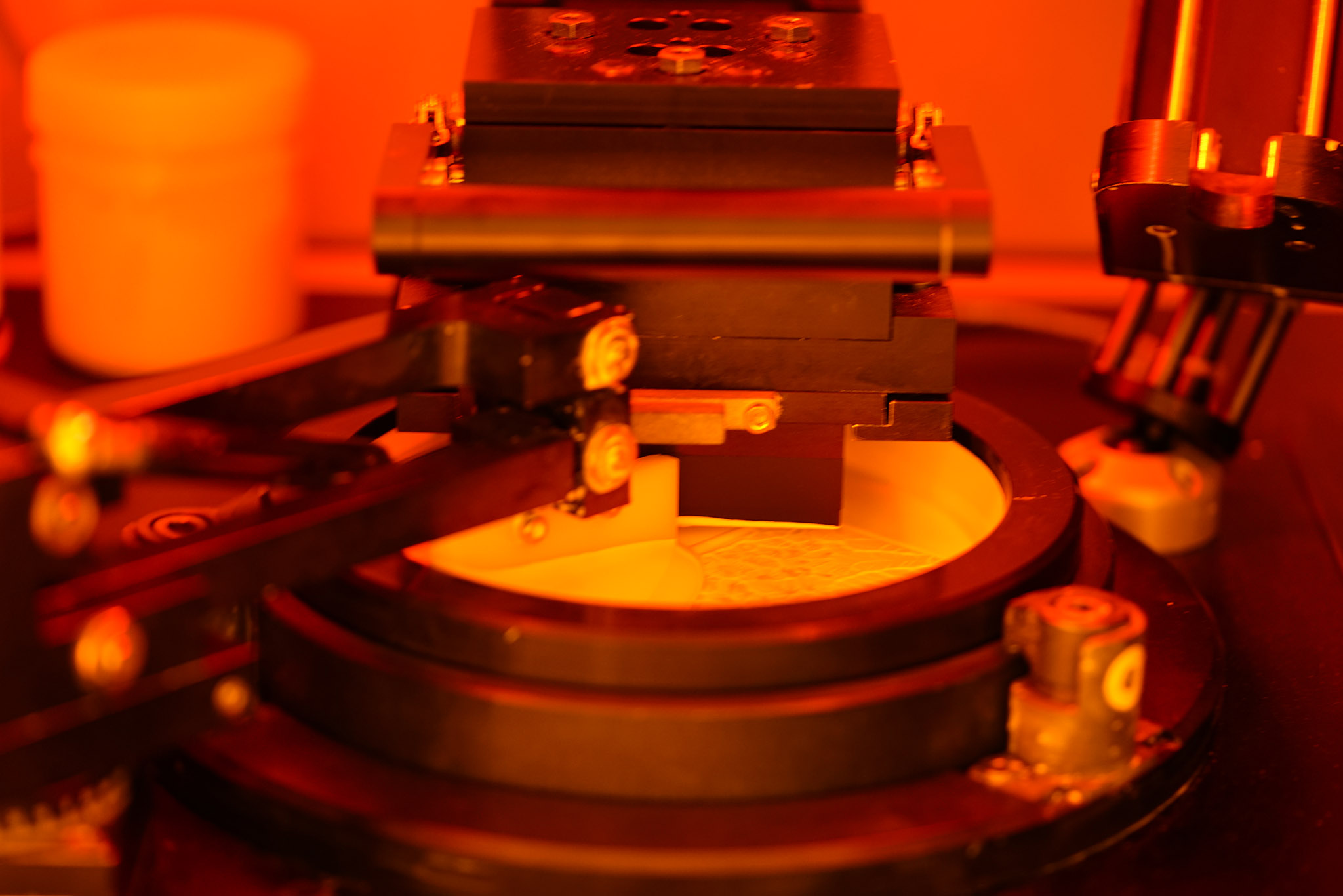
Tassilo Moritz: Yes, indeed, ”CerAM VPP”, or Vat Photopolymerization proved to be a hit. This is an additive manufacturing method in which monomers – short plastic molecules – are cured by light. Specifically, it looks like this: We coat the bottom of a transparent tub with a thin layer of a glass powder monomer suspension.
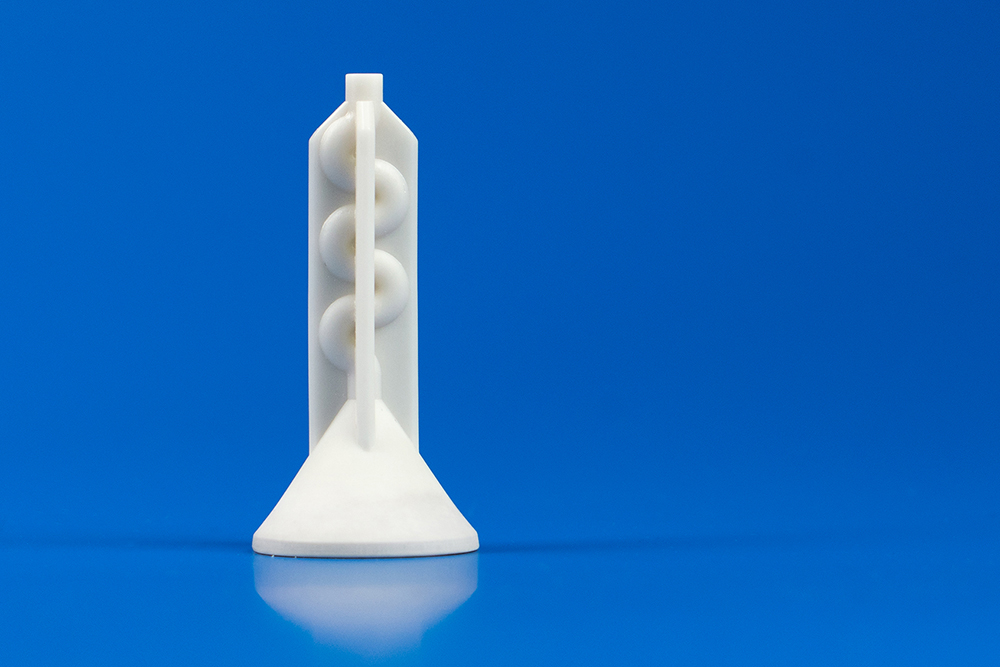
From below, a projector uses ”direct light processing” to illuminate the layer through the bottom of the tub with a specific wavelength of light and cures the monomers at the desired points, as is familiar from plastic fillings at the dentist. Then, a platform lifts the just created component layer a little bit, the next suspension layer is painted on the bottom of the tub, the platform lowers again to contact the suspension, the layer is illuminated again. This process is repeated until the green body is ready. This has shown that with this approach, more complex structures can be created – more curvatures and channels – than with the traditional manufacturing process, which leads to a higher amplification effect. In the future, this will enable us to manufacture much better and more accurate photomultipliers than before.
Rolf-Jürgen Ahlers: I can only underline that. With the new approach, we are no longer limited by our design. Rather, we can design the geometry in such a way that we achieve the optimum in terms of how a photomultiplier works. Specifically, we can further increase the intensity and low noise of the sensor.
Is the process suitable for industry, considering the speed at which a component is printed?
Jochen Schilm: Plants with larger tubs and working areas are already under development. Several components can be produced on these at once, which will also drastically reduce the production time per part. This will enable speeds that were previously reserved for injection molding only.
Rolf-Jürgen Ahlers: You also have to remember: We are not about mass products. We produce small batches that we repeatedly adapt to the very different wishes of our customers. That's why this additive process is likely to give us exactly the flexibility we were looking for. As a result, smaller series will also be profitable for users.
What process engineering hurdles had to be overcome in adapting CerAM VPP? Certainly, it cannot be transferred 1:1 from ceramic to glass.
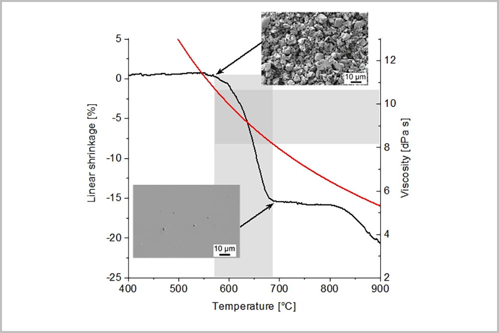
Jochen Schilm: Since the glass particles in the suspension are transparent in contrast to ceramic particles, we had to adjust the illumination parameters. The most challenging part, however, was to adjust the optimal sintering process so that a dense component would be produced in the end. The glass particles must only soften slowly, but not start to melt. This would cause the components to deform or the component edges to become rounded.
What new applications could you potentially open up by using this process?
Rolf-Jürgen Ahlers: In the future, photomultipliers could be used in wastewater treatment plants, for example, to measure how heavily the wastewater is contaminated with hormones, antibiotics or other problematic organic substances. I also see a lot of potential in aerospace, environmental technology, medical technology, the food industry and many other sectors.
Tassilo Moritz: It would also be imaginable to combine different medical examination methods, such as MRI with tumor markers.
What will happen next? Will ProxiVision be using this additive manufacturing process in production in the near future?
Tassilo Moritz: We're not quite there yet. It will certainly take another year and a half before we reach this point. Until then, we still have to optimize the process in terms of production technology. In addition, we could also investigate in a project how production could be supplemented by further manufacturing steps, such as laser processing or laser soldering.
Rolf-Jürgen Ahlers: For example, one can also think of coatings, electrically conductive glass or integrated resistors. In general, I see good opportunities for opening up completely new fields of application for photomultipliers in the future with this approach.
|
Further information:
- Fraunhofer IKTS department "Processes and Components"
- Fraunhofer IKTS group "Joining Technology"
- How glass learns to illuminate itself and create heat
Stay informed: You are welcome to subscribe to our newsletter, read our other blog articles and follow us on LinkedIn, Instagram and YouTube.
