 Fraunhofer Institute for Ceramic Technologies and Systems IKTS
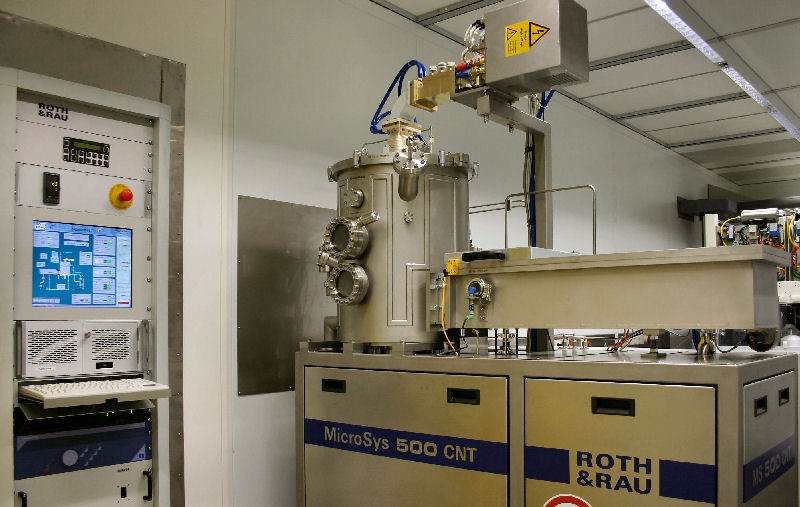
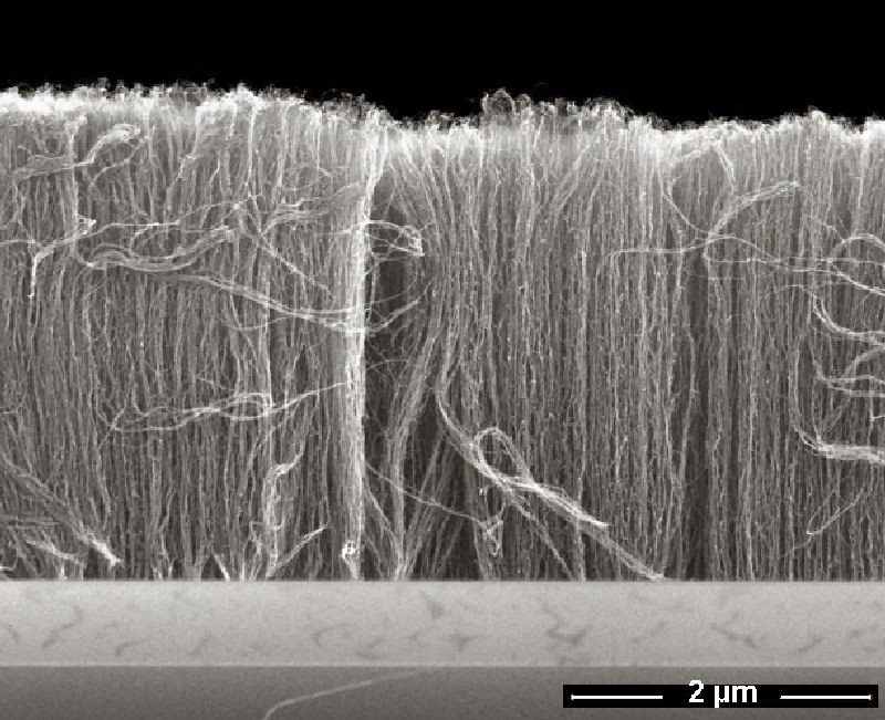
Since the discovery of carbon nanotubes (CNT) in 1991 a lot of efforts were made by scientists all over the world to use the potential of CNT for numerous applications. The outstanding properties of carbon nanotubes can be attributed to the combination of high mechanical strength, high thermal and electrical conductivity and good chemical resistance. Due to their small diameter of some nanometers compared to their length up to several millimeters it is easy to realize aspect ratios > 10 000. With these characteristics they are suited for applications in the field of sensors and actuators as well as for field emitters, semiconductor devices and for energy storage. Carbon nanotubes can basically be manufactured as undirected volume material or fixed on substrates. In the second case it is the aim to manufacture vertically aligned carbon nanotubes.
At Fraunhofer IKTS vertically aligned layers of multi-walled carbon nanotubes (MWCNT) as well as single-walled carbon nanotubes (SWCNT) are deposited on different substrates. Two CVD deposition systems are available for CNT synthesis. Fraunhofer IKTS offers a closed process chain for layers of aligned carbon nanotubes, comprising the selection of suitable carrier materials and catalyst systems as well as synthesis, characterization and further processing of CNT structures.
Products and services offered
- Manufacturing of aligned and non-aligned CNT layers on defined substrates
- Preparation and development of catalysts suitable for carbon nanotube growth
- Carbon nanotube synthesis on substrates with diameters of up to 100 mm (4 inch) or on custom-specific substrate geometries
- Preparation of structured carbon nanotube layers
- CNT growth on electrical conductive substrates
- Complex characterization (spectroscopic, microscopic)
- Preparation and development of prototypes with nanotube structures
Technical equipment
- PECVD equipment „MicroSys 500“ (Roth & Rau)
- LPCVD laboratory system