To measure the electrical properties of high-performance electronics, which must withstand harsh environmental conditions and still be durable, the IKTS group "System Integration and AVT" offers the following measurements tailored to customer requirements from one single source.
Electrical Special Measurement Methods for High-Performance Electronics
Topic
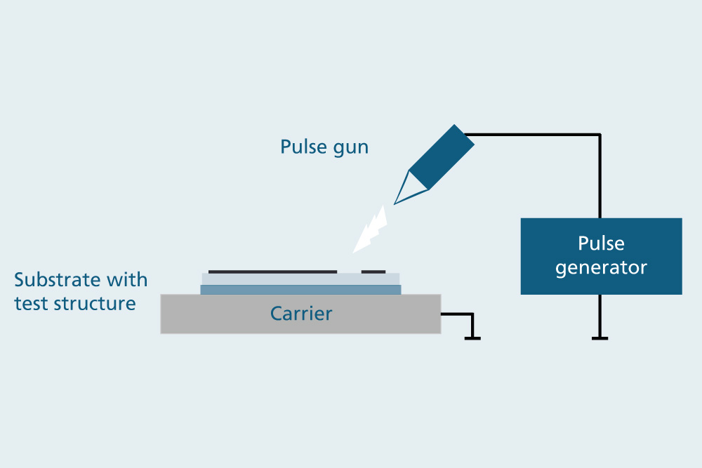
Measuring electrostatic discharge (ESD)
Depending on their design, construction and size, electronic components and assemblies are susceptible to damage caused by electrostatic discharge (ESD). Frictional electricity causes accumulations of charge carriers at interfaces during ESD, resulting in potential differences. In addition to active silicon devices, this effect can damage thick-film components (for example, thick-film resistors).
To investigate the reliability and determine the failure probability of such components and assemblies, the IKTS group "System Integration and AVT" uses ESD measurements: Electrostatic discharge is simulated in a targeted manner. Thick-films, components and systems are tested by means of single or paired pulses. The changes before and after the electrostatic discharge are compared and interpreted to derive optimization needs for high-performance electronics.
Partial discharge measurement behavior of insulators
Wiring carriers are used in the construction of electronic assemblies. Further components are mounted on them. The wiring carrier acts as an insulating mechanical support. It carries the required conductor pattern and has the mounting locations. Its quality is determined by its insulation system. It can be measured non-destructively by means of short-term partial discharge. The partial discharge measurements are always performed below the breakdown voltage and under defined conditions so that the component is not damaged.
Partial discharge measurement is well established for describing the behavior of insulation materials in high-voltage test engineering. The IKTS group "System Integration and AVT" has now adapted the method to describe the behavior of the wiring carriers of high-performance electronics.
Breakdown voltage measurement
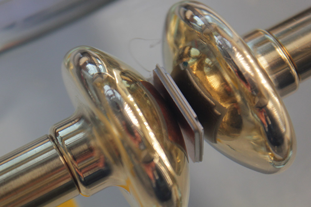
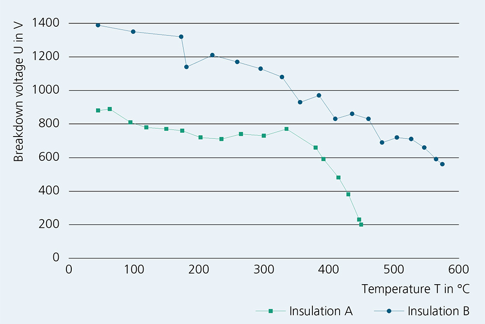
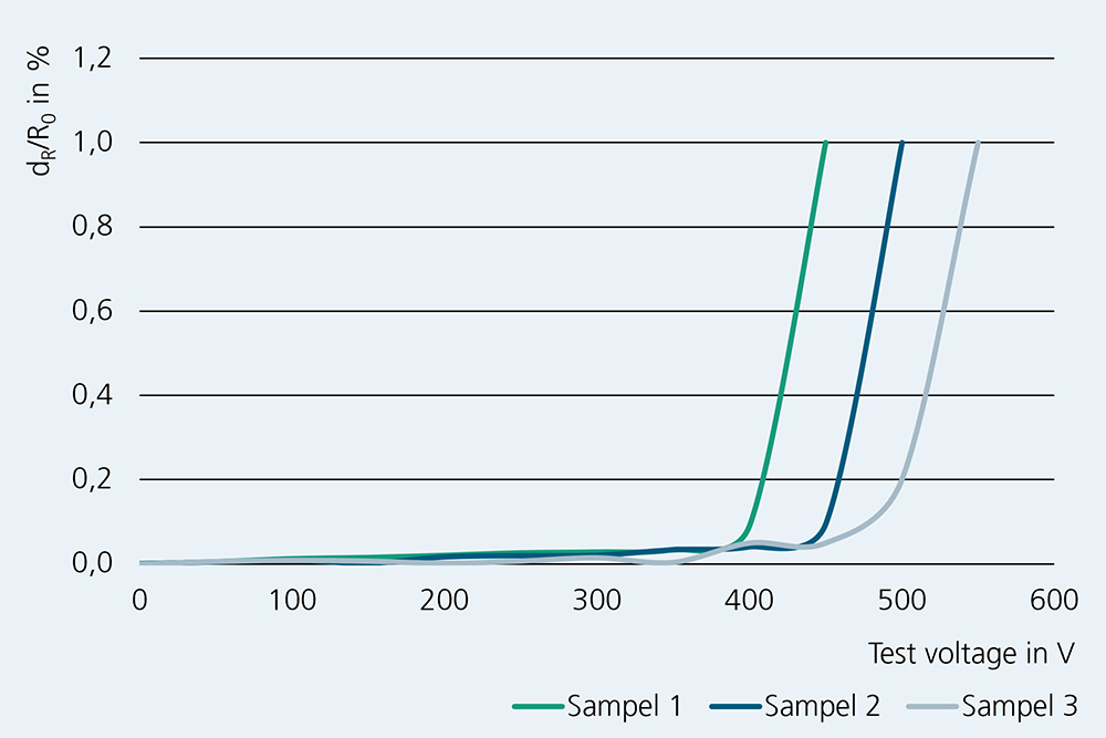
The dielectric strength of an insulating material corresponds to the maximum permissible electric field strength that may be applied to an insulator before electrical breakdown occurs and the insulator is thus damaged. This value must be determined both for insulating wiring carriers and for the thick-film-based dielectrics used. For this purpose, the IKTS group "System Integration and AVT" has developed a method for high-performance electronics, which it offers inline with customer requirements.
During the measurement, the test samples are positioned between two adjacent electrodes. The applied test voltage is continuously increased until the dielectric strength is reached and a breakdown occurs. The breakdown voltage depends on various conditions. For example, it can be determined as a function of temperature. The tested temperature range is typically between -60 and 900 °C
Insulation resistance measurement
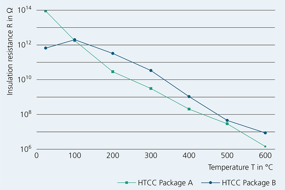
The insulation resistance of wiring supports and dielectric layers is determined by insulation strength measurements. During the measurement, the test samples are clamped between two applied electrodes. The applied test voltage is continuously increased. The insulation resistance recorded in this way depends on various conditions. For example, it can be determined as a function of temperature.
The IKTS group "System Integration and AVT" offers insulation resistance measurements for high-performance electronics under specifically defined conditions in a temperature range between -60 and 900 °C.
Short term overload (STOL) measurement
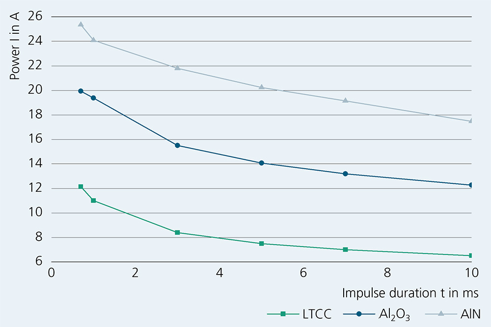
An important parameter for thick-film resistors is the maximum permissible power dissipation density that may be applied across the resistor. It is measured in watts per unit area. Above the permissible power dissipation density, the thick-film resistor is irreversibly damaged.
The IKTS group "System Integration and AVT" calculates the power dissipation density of thick-film resistors and other components of high-power electronics via "Short Term Overload (STOL)".
In the measurement, the samples are sufficiently electrically and thermally contacted on a test set-up and selectively subjected to an electrical power dissipation: The sample is heated, and the heating is documented. After a specified time, the power dissipation is switched off. The sample cools down. The electrical cold resistances of the sample before and after heating are compared.
This procedure is repeated with a power dissipation increased by a factor of X until the cold resistance only changes by a defined value (usually 0.1 %). This value signals the damage limit. Due to the sample geometry, the electrical parameters are linked to the geometrical parameters and the maximum permissible power loss density can be calculated at this point.
Current carrying capacity measurement
In current-carrying capacity measurements, e.g. of thick-film conductors, material characteristics, specimen geometry and measurement setup are combined. On the one hand, the targeted heating of the samples is recorded, which results from the concrete power application. On the other hand, the geometrical conductor tensile parameters (conductor tensile cross-sections) are determined in order not to exceed specified loss temperatures during power application.
During the measurement, the samples are contacted at a defined temperature on the measuring device so that the test structures can subsequently be subjected to predetermined power losses in a user-specific manner. The heating of the test structures can be detected by infrared measurement or the pyrometer and evaluated with a resistance thermometer. The combination of the electrical, geometrical and thermal parameters enables specific statements to be made on the current-carrying capacity of the conductor runs. Furthermore, critical occupancy densities of the conductor runs can be detected and the quality of the thermal connections can be characterized. In addition, current-carrying capacity measurements are used to ensure active aging of the specimens by "power cycling".
