Fraunhofer Institute for Ceramic Technologies and Systems IKTS
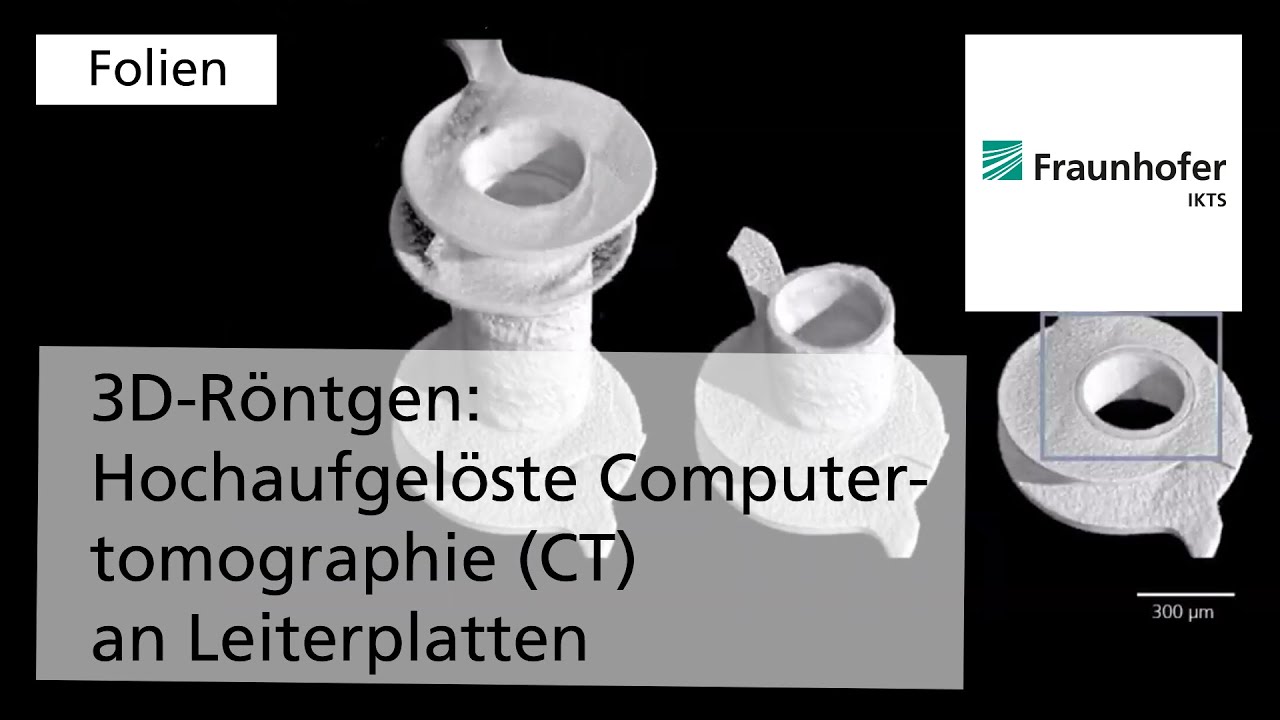
Flat assemblies such as electronic circuit boards can only be examined with insufficient resolution due to their usually large sample geometry. The distance between the X-ray source and the sample is usually too great to examine small sub-areas more closely and to detect the smallest defects such as cracks or pores in solder connections (BGA, QFN, QFP).
Fraunhofer IKTS offers a special X-ray tomography method for this task, which can analyze sub-areas of large-area circuit carriers such as printed circuit boards in high resolution and non-destructively.