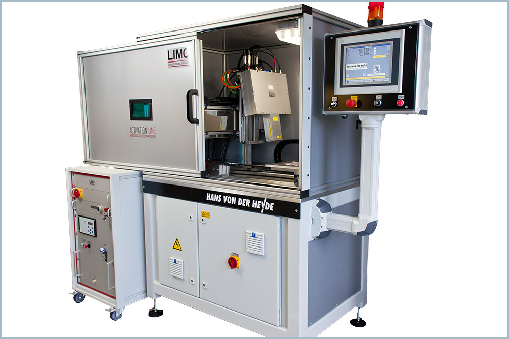
Fraunhofer IKTS is investigating laser-based approaches for post-processing of wet-chemical metallic and ceramic layers on a broad range of substrates. It enables the removal of the organic phase and sintering/melting of the printed layers in air, all without substantial thermal damage to the substrates. To achieve this, we use high-power diode laser (HPDL) array generating line-shaped beam that is swept over the printed structures.
Specifications
- Line-shaped laser beam profile: 30 mm long line
- Continuous-wave operation mode, optical power up to 1000 W, wavelength of 980 nm
- Processing speed: 0.01-60 m/min (corresponds to dwell time on the millisecond scale)
- Processing area: up to 250 mm x 300 mm
- Processing in air or in protective gas (N2, Ar) in case of especially reactive materials
Key features of the technology
- Selectivity: only printed layers absorb the laser radiation and are heated selectively in case of transparent substrates
- High-speed: achieving low electrical resistivity in printed structures based on non-noble metals by processing in air, minimizing thermal damage to thermally sensitive substrates, high productivity (roll-to-roll compatibility)
- Energy efficiency: electro-optical conversion efficiency of 50 % to 60 %
Components demonstrated by combining wet-chemical deposition and HPDL
- Metallic interconnects, sensor structures on flexible thermally sensitive substrates: Ag, Au, Pt, Cu, Bi, Fe-Ni alloys
- Metallic interconnects, sensor structures on ceramic substrates: Pt, PtRh, Mo
- Sealing layers on porous oxide ceramic matrix composite materials
Services offered
- Realizing customer-specific structures on a broad range of substrates
- Flexible: polymer tapes, paper, glass/ceramic/metallic tapes, metallic/ceramic fleece/foam
- Rigid: glass, ceramics including ceramic matrix composites, Si-wafers
- Tailoring of laser sintering parameters to customer-specific structures prepared by inkjet-, aerosol jet-, screen-, dispenser-printing, or wet-powder spraying
- Determining microstructure and properties (e.g. electrical resistivity) of the layers in relation to their printing and laser processing parameters
- Know-how in the laser sintering of commercially available and Fraunhofer IKTS proprietary inks
- Partnership in collaborative research projects, performing feasibility studies, preparing prototypes and demonstrators
