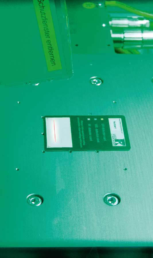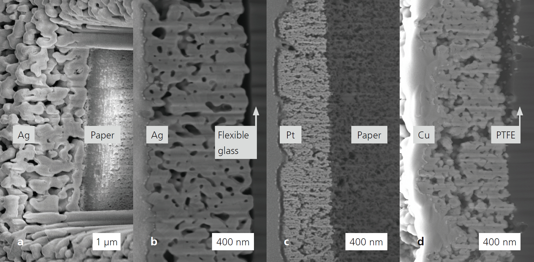

Realizing high-quality inkjet-printed metal structures on large-area thin (100–200 μm) and ultrathin (< 10 μm) substrates enables a wide range of applications for flexible electronics. Thermal post-processing of inkjet-printed structures in a belt furnace for approx. 30–60 minutes at temperatures of at least 130 °C for silver, or more than 300 °C for copper and gold, is usually required to remove organic components, sinter the metal particles and enable electrical conductivity. This critical technological step is determined by the selection and properties of the printed materials and is very time-consuming. Furthermore, it requires high investment costs for furnace technology. An alternative approach to post-processing, based on a micro-optically designed one-dimensional diode laser source (diode laser array) with a line-shaped beam profile and high energy input, opens up new possibilities in the field of printed electronics. Using this innovative approach, Fraunhofer IKTS was able to sinter a broad range of materials in an extremely short time. The substrate is moved forward continuously with a speed of 5–20 m/min (R2R compatible) during this process. IKTS has a broad portfolio of specially developed water-based metal nanoinks (Ag, Cu, Au and Pt), which are used for laser sintering. To demonstrate the performance of the method, the metal conducting paths were inkjet-printed onto different thin (glass, 100 μm; PET, 120 μm; paper, 170 μm) and ultrathin (PET, < 10 μm) substrates. The printed structures of silver, gold and platinum showed moderate electrical conductivity already after drying. Subsequently, a few milliseconds of laser processing led to a drastic improvement of electrical conductivity, so that silver conducting paths showing an electrical resistivity three times that of the bulk silver were realized, even on ultrathin 2.5 μm PET substrates. This deviation from the bulk resistivity is due to the residual porosity (30–40 vol %) of the printed layers. In case of copper, gold and platinum structures, the new technique also yielded an improved resistivity, which was higher by the factor 10 compared to the values of the bulk material. In addition to the electrical conductivity, the mechanical bending ability of the structures was tested as well. The silver conducting paths printed on paper were successfully tested down to radii as small as 4 mm. The 100-cycle test with a bending radius of 10 mm resulted only in negligible changes (< 1 %) in the resistance values of the samples. Thus, the laser-based ultrafast heat treatment can be used for post-processing even of materials which are high-melting and difficult to sinter. This key technology paves the way for the use of new classes of materials in printed electronics on thermally sensitive substrates.
This work was supported by the Fraunhofer Attract INNOVELLE project.