 Fraunhofer Institute for Ceramic Technologies and Systems IKTS
Highly thermally conductive silicon nitride ceramics for power electronics
Current research
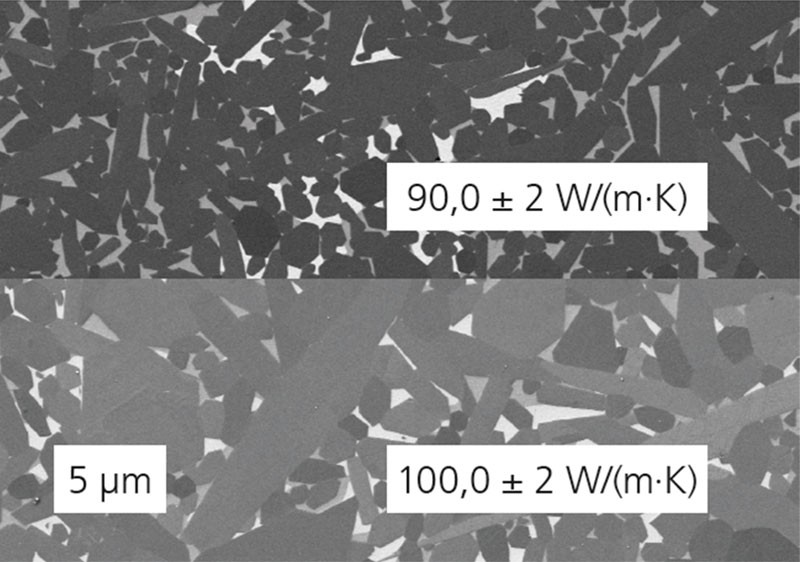
Microstructure before (left) and after (right) optimization of the sinter process.
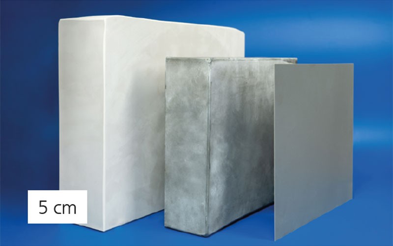
Green and sintered bodies made of Si3N4 and 320 μm substrate produced from them through multi-wire sawing.
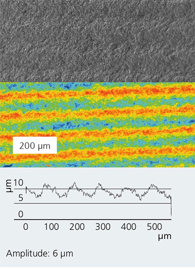
Laser scanning microscope image (left) and FESEM image (right) of the Si3N4 substrate surface after sawing.
Silicon nitride (Si3N4) materials are characterized by excellent mechanical and tribological properties even at high temperatures. In addition, the thermal conductivity of Si3N4 can be increased to up to 100 W/(m∙K) by adjusting the chemical composition and microstructure. This combination of high strength and good thermal conductivity is unique and leads to a very high thermal cycling stability and long working life of Si3N4-based substrates. Fraunhofer IKTS uses these properties combined with the high electrical resistance and the voltage stability of the material in the BMWK project CuSiN (FKZ 3ETE025), which aims to develop active metal-brazed copper silicon nitride composites (AMB substrates) for use as reliable circuit carriers in power electronics.
The effect of the type and quantity of oxide additives as well as of Si3N4 powder qualities was investigated by adapting the materials on the laboratory scale. Materials with thermal conductivities of > 90 W/(m∙K) could be realized from cost-efficient Si3N4 powders with low oxygen content and reduced aluminum impurities.
The granule composition developed on the laboratory scale was transferred to pilot scale (10 kg scale). The researchers used the granules, which have good pressing ability, to produce blocks through uniaxial or cold isostatic pressing with dimensions of 320 x 230 x 45 mm and 265 x 195 x 60 mm. The sintering of large blocks requires that temperature gradients which occur during heating and cooling be taken into account. Using modeling, it was possible to estimate critical stresses during the sintering process and optimize sintering. Fraunhofer CSP Halle produced 7.5 x 5.5 inch substrates from the sintered blocks through multi-wire sawing. The substrates thus obtained are of low roughness and high flatness; they do not require any mechanical post-processing of the substrate surface and allow for precise adjustment of the substrate thickness from e.g. 320 μm down to 100–150 μm.
In addition to developing the AMB technology, the team also qualified the methods for characterizing the substrates in terms of microstructure, thermal, mechanical, electrical, and dielectric properties.
Further optimization of the material and the sintering regime will put thermal conductivities of > 100 W/(m∙K) within reach.
Services offered
- Application-oriented development of nitridematerials
- Characterization of substrates with regard to mechanical, thermal and electrical properties