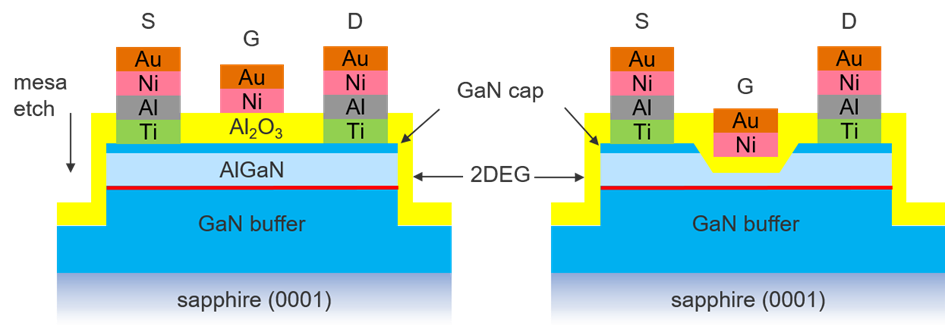
Thin-film technologies such as atomic layer deposition (ALD) play a significant role in the ongoing miniaturization in the semiconductor industry. This technology enables 3D structures to be deposited and layer thicknesses to be precisely adjusted. In the current "ALEStar" project, ALD processes are to be combined with novel etching processes such as atomic layer etching (ALE) to realize nitride devices with precisely tunable electrical properties. Compared to silicon, nitride semiconductor materials, such as gallium nitride (GaN), aluminum nitride (AlN) and their ternary compounds AlGaN, are characterized by high electron mobility, breakdown voltage and a large direct band gap. Therefore, nitride semiconductor materials are particularly suitable for high-frequency applications and high-voltage electronics.
ALE technology offers two major advantages to increase efficiency in the fabrication of high performance nitride devices. On the one hand, the atomic layer precise ALE process allows a more accurate fabrication of the very low step heights especially in the contact and gate area with simultaneously reduced damage compared to previous dry chemical etching processes such as Rapid Ion Etching (RIE). On the other hand, the self-limitation of the process promises high lateral homogeneity over the entire wafer. In addition, the researchers are looking into the possibility of in-situ passivation of the etched layer by depositing thin film dielectrics. The process development is supported by an accompanying characterization of the materials used. In addition, the surface condition of the test components after processing as well as their functionality will be investigated. This enables monitoring of the etching process at an early stage of development.
Another focus of the project is the evaluation of etching gases. The aim is to examine what alternatives there are to chlorine-containing etching gases and what environmental and technical advantages are associated with them.


