Fraunhofer Institute for Ceramic Technologies and Systems IKTS
The "Nanoscale Materials and Analysis" group at Fraunhofer IKTS uses high-resolution electron and ion microscopy, X-ray techniques, and methods for determination of nanomechanical properties for multiscale and multiphysical materials characterization as well as evaluation and analysis of material states.
The existing electron microscopy methods are employed in the imaging and high-resolution analysis of various materials and components to answer the following questions:
- What is the elemental composition of the deposit on the metal-ceramic interface?
- How large are the mechanical stresses in a silicon substrate adjacent to a Cu TSV?
- Does a deposition process function for thin films (thickness, morphology) or a TSV (complete filling, pores)?
- How are the phases arranged three-dimensionally in the material?
- How do filter materials differ in terms of their pore size distributions and what does the three-dimensional pore network look like?
- How does a dielectric material in a microchip fail?
- What are the dimensions of nanostructures, are they crystalline, and how are they oriented?
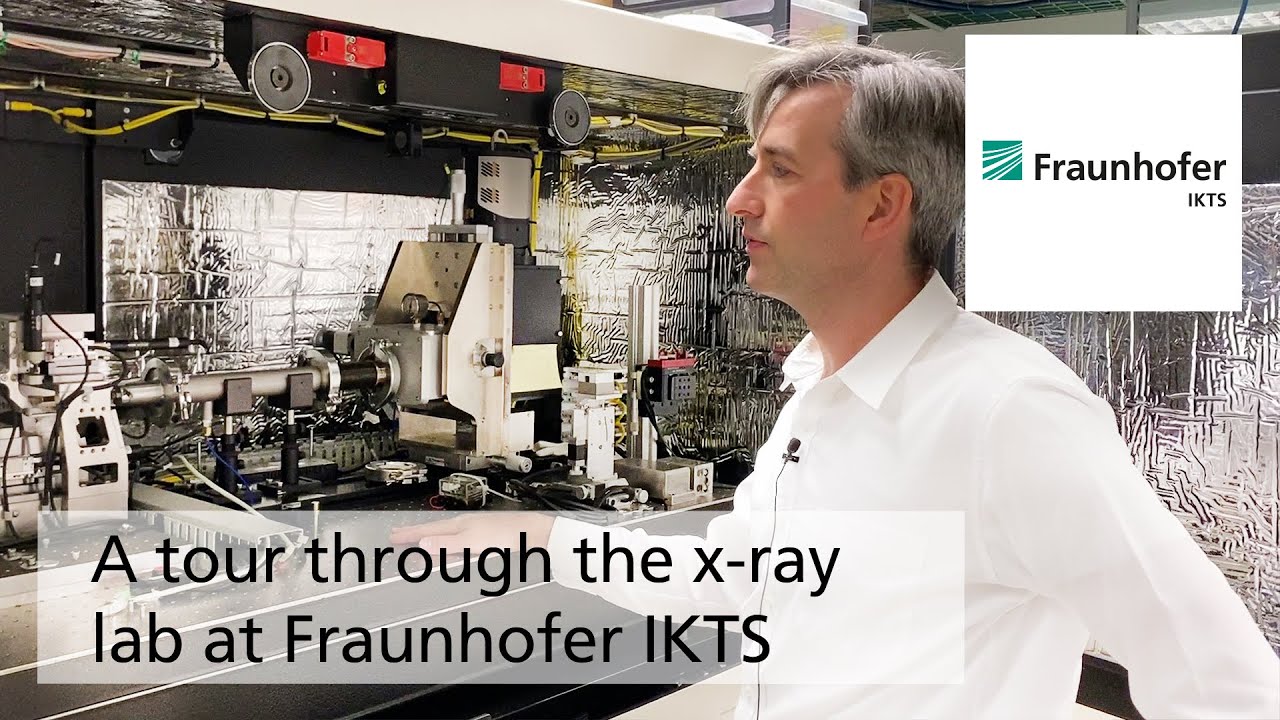
X-ray microscopy/X-ray nanotomography
At Fraunhofer IKTS, X-ray microscopy and a technique based on it, X-ray nanotomography, are used to analyze structures and defects in materials. This enables non-destructive examination of structural and functional materials at the microscopic level with a resolution of about 50 nm.
The main applications lie in visualization of pores, inclusions, and cracks in composite materials (e.g., ceramic matrix composites), nanoporous materials (filter membranes), and microelectronics (through silicon vias, or TSVs).
Development of test technology and methods for micro- and nanostructures
Novel materials and production technologies in thin-film and nanotechnology as well as for biological and medical applications call for new test methods.
The "Nanoscale Materials and Analysis" group at Fraunhofer IKTS possesses a unique infrastructure offering a wide range of high-resolution microscopy methods and continuously develops innovative theoretical, experimental, and technology-oriented methods and equipment to meet the demanding requirements of emerging fields such as nanotechnology.
With the combination of various technologies and in-depth process and methods know-how, it is possible to solve challenging tasks that could not be accomplished using one characterization technology alone.
Services offered
- Target preparation in specimens of components and assemblies for microscopic examination (mechanical, wet chemical, and FIB methods)
- High-resolution scanning electron microscopy (FESEM) and elemental analysis (EDX)
- Potential contrast microscopy
- Circuit modification (FIB and Pt deposition)
- FIB tomography
- Ultrahigh-resolution transmission electron microscopy (TEM and STEM)
- Elemental analysis in TEM (EDX and EELS)
- Internal stress measurements in TSV environment
- Nanostructure, nanoindentation and tensile tests in TEM
- Imaging and analysis in TEM up to 400 °C
- X-ray microscopy, X-ray tomography, and X-ray laminography to a resolution of 50 nm, optionally at elevated temperatures and in protective gas atmospheres, in-situ reaction chambers, and micromechanical experiments (indentation, double cantilever beam test)
- Development and characterization of novel X-ray optics (multilayer Laue lenses, or MLLs) for X-ray microscopy
- Optimization of imaging methods and algorithms